AD9776A/AD9778A/AD9779A
Rev. B | Page 50 of 56
SYNCHRONIZING DEVICES TO A SYSTEM CLOCK
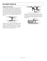
The AD9776A/AD9778A/AD9779A offer a pulse mode synchro-
nization scheme (see Figure 89) to align the DAC outputs of
multiple devices within a system to the same DACCLK edge.
The internal clocks are synchronized by providing either a one-
time pulse or a periodic signal to the SYNC_I inputs (,
SYNC_I−). The SYNC_I signal is sampled by the internal
DACCLK sample rate clock.
The SYNC_I input frequency has the following constraint:
f
SYNC_I
≤
f
DATA
When the internal clocks are synchronized, the data-sampling
clocks between all devices are phase aligned. The data input
timing relationships can be referenced to either REFCLK or
DATACLK.
For this synchronization scheme, all devices are slave devices,
and the system clock generation/distribution chip serves as the
master. It is vital that the SYNC_I signal be distributed between
the DACs with low skew. Likewise, the REFCLK signals must be
distributed with low skew. Any skew on these signals between the
DACs must be accounted for in the timing budget. Figure 89
shows an example clock and synchronization input scheme.
Figure 90 shows the timing of the SYNC_I input with respect to
the REFCLK input. Note that although the timing is relative to
the REFCLK signal, SYNC_I is sampled at the DACCLK rate.
This means that the rising edge of the SYNC_I signal must occur
after the hold time of the preceding DACCLK rising edge, not
the preceding REFCLK rising edge.
INTERRUPT REQUEST OPERATION
The IRQ pin (Pin 71) acts as an alert in the event that the
device has a timing error and should be queried (by reading
Register 0x19) to determine the exact fault condition. The IRQ pin
is an open-drain, active low output. The IRQ pin should be pulled
high external to the device. This pin can be tied to the IRQ pins
of other devices with open-drain outputs to wire-OR these pins
together.
There are two different error flags that can trigger an interrupt
request: a data timing error flag or a sync timing error flag. By
default, when either or both of these error flags are set, the IRQ pin
is active low. Either or both of these error flags can be masked
to prevent them from activating an interrupt on the IRQ pin.
The error flags are latched and remain active until the interrupt
register, Register 0x19, is either read from or the error flag bits
are overwritten.
SYSTEM CLOCK
LOW SKEW
CLOCK DRIVER
LOW SKEW
CLOCK DRIVER
MATCHED
LENGTH TRACES
REFCLK
SYNC_I
REFCLK
SYNC_I
OUT
OUT
MATCHED
LENGTH TRACES
PULSE
GENERATOR
06
45
2-
31
1
Figure 89. Multichip Synchronization in Pulse Mode
DACCLK
REFCLK
SYNC_I
t
S_SYNC
t
H_SYNC
06
45
2-
31
2
Figure 90. Timing Diagram of SYNC_I with Respect to REFCLK When Synchronizing Multiple Devices to Each Other

