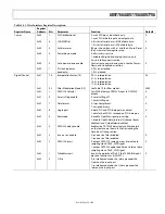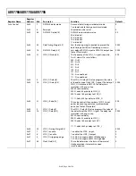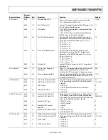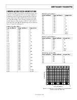
AD9776A/AD9778A/AD9779A
Rev. B | Page 27 of 56
SERIAL INTERFACE PORT PIN DESCRIPTIONS
Serial Clock (SCLK)
The serial clock pin synchronizes data to and from the device
and controls the internal state machines. The maximum frequency
of SCLK is 40 MHz. All data input is registered on the rising edge
of SCLK. All data is driven out on the falling edge of SCLK.
Chip Select (CSB)
Active low input starts and gates a communication cycle. It
allows more than one device to be used on the same serial
communication lines. The SDO and SDIO pins go to a high
impedance state when this input is high. Chip select should
stay low during the entire communication cycle.
Serial Data I/O (SDIO)
Data is always written into the device on this pin. However, this
pin can be used as a bidirectional data line. The configuration
of this pin is controlled by Register 0x00, Bit 7. The default is
Logic 0, configuring the SDIO pin as unidirectional.
Serial Data Out (SDO)
Data is read from this pin for protocols that use separate lines
for transmitting and receiving data. In the case where the device
operates in a single bidirectional I/O mode, this pin does not
output data and is set to a high impedance state.
MSB/LSB TRANSFERS
The serial port can support both MSB-first and LSB-first data
formats. This functionality is controlled by the LSB-/MSB-first
register bit (Register 0x00, Bit 6). The default is MSB-first format
(LSB/MSB first = 0).
When MSB-first format is selected (LSB/MSB first = 0), the
instruction and data bit must be written from MSB to LSB.
Multibyte data transfers in MSB-first format start with an
instruction byte that includes the register address of the most
significant data byte. Subsequent data bytes should follow from
high address to low address. In MSB-first mode, the serial port
internal byte address generator decrements for each data byte of
the multibyte communication cycle.
When LSB/MSB first = 1 (LSB first) the instruction and data
bit must be written from LSB to MSB. Multibyte data transfers
in LSB-first format start with an instruction byte that includes
the register address of the least significant data byte, followed by
multiple data bytes. The serial port internal byte address genera-
tor increments for each byte of the multibyte communication cycle.
The serial port controller data address decrements from the data
address written toward 0x00 for multibyte I/O operations if the
MSB-first format is active. The serial port controller address
increments from the data address written toward 0x1F for
multibyte I/O operations if the LSB-first format is active.
R/W N1 N0 A4 A3
A2 A1 A0 D7 D6
N
D5
N
D0
0
D1
0
D2
0
D3
0
D7 D6
N
D5
N
D0
0
D1
0
D2
0
D3
0
INSTRUCTION CYCLE
DATA TRANSFER CYCLE
CSB
SCLK
SDIO
SDO
06
45
2-
05
0
Figure 53. Serial Register Interface Timing, MSB First
A0 A1 A2 A3 A4
N0 N1 R/W D0
0
D1
0
D2
0
D7
N
D6
N
D5
N
D4
N
D0
0
D1
0
D2
0
D7
N
D6
N
D5
N
D4
N
INSTRUCTION CYCLE
DATA TRANSFER CYCLE
CSB
SCLK
SDIO
SDO
06
45
2-
05
1
Figure 54. Serial Register Interface Timing, LSB First
INSTRUCTION BIT 6
INSTRUCTION BIT 7
CSB
SCLK
SDIO
t
DS
t
DS
t
DH
t
PWH
t
PWL
t
SCLK
06
45
2-
05
2
Figure 55. Timing Diagram for 3-Wire Interface Register Write
DATA BIT n – 1
DATA BIT n
CSB
SCLK
SDIO
SDO
t
DV
0
64
52
-0
53
Figure 56. Timing Diagram for 3-Wire Interface Register Read


