AD9776A/AD9778A/AD9779A
Rev. B | Page 39 of 56
SOURCING THE DAC SAMPLE CLOCK
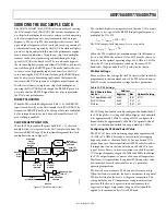
The AD9776A/AD9778A/AD9779A offer two modes of sourcing
the DAC sample clock (DACCLK). The first mode employs an
on-chip clock multiplier that accepts a reference clock operating
at the lower input frequency, most commonly the data input
frequency. The on-chip PLL then multiplies the reference clock
up to a higher frequency, which can then be used to generate all
of the internal clocks required by the DAC. The clock multiplier
provides a high quality clock that meets the performance require-
ments of most applications. Using the on-chip clock multiplier
removes the burden of generating and distributing the high
speed DACCLK at the board level. The second mode bypasses
the clock multiplier circuitry and allows DACCLK to be directly
sourced through the REFCLK pins. This mode enables the user
to source a very high quality input clock directly to the DAC
core. Sourcing the DACCLK directly through the REFCLK pins
may be necessary in demanding applications that require the
lowest possible DAC output noise at higher output frequencies.
In either case (that is, using the on-chip clock multiplier or
sourcing the DACCLK directly though the REFCLK pins), it is
necessary that the REFCLK signal have low jitter to maximize
the DAC noise performance.
DIRECT CLOCKING
When the PLL is disabled (Register 0x09, Bit 7 = 0), the REFCLK
input is used directly as the DAC sample clock (DACCLK). The
frequency of REFCLK needs to be the input data rate multiplied
by the interpolation factor (and by an additional factor of 2 if
zero stuffing is enabled).
CLOCK MULTIPLICATION
When the PLL is enabled (Register 0x09, Bit 7 = 1), the clock
multiplication circuit generates the DAC sample clock from the
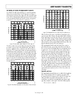
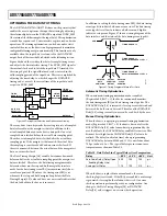
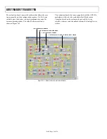
lower rate REFCLK input. The functional diagram of the clock
multiplier is shown in Figure 72.
ADC
PHASE
DETECTOR
VCO
LOOP
FILTER
PIN 65 AND
0x00[1]
PLL LOCK
DETECT
REFCLK
(PIN 5,
PIN 6)
0x0A[7:5]
PLL CONTROL
VOLTAGE
0x09[7]
PLL ENABLE
DACCLK
DATACLK OUT
(PIN 37)
0x01[7:6]
INTERPOLATION
FACTOR
0x09[6:5]
PLL VCO
DIVISOR
0x09[4:3]
PLL LOOP
DIVISOR
÷IF
÷N
2
÷N
1
0x08[7:2]
VCO BAND
SELECT
06
45
2-
0
92
Figure 72. Clock Multiplier Circuit
The clock multiplier circuit operates such that the VCO outputs
a frequency, f
VCO
, equal to the REFCLK input signal frequency
multiplied by N1 × N2.
)
(
N2
N1
f
f
REFCLK
VCO
×
×
=
The DAC sample clock frequency, f
DACCLK
, is equal to
N2
f
f
REFCLK
DACCLK
×
=
When the PLL is enabled, the maximum input clock frequency
f
REFCLK
is 250 MHz. The values of N1 and N2 must be chosen to
keep f
VCO
in the optimal operating range of 1.0 GHz to 2.0 GHz.
Once the VCO output frequency is known, the correct PLL
band select (Register 0x08, Bits[7:2]) value can be chosen.
PLL Bias Settings
There are three bias settings for the PLL circuitry that should be
programmed to their nominal values. The PLL values shown in
Table 22 are the recommended settings for these parameters.
Table 22. PLL Settings
PLL 3-Wire Interface
Control
Address
Optimal Setting
Register Bits
PLL Loop Bandwidth
0x0A
[4:0]
01111
PLL VCO Drive
0x08
[1:0]
11
PLL Bias
0x09
[2:0]
011
The PLL loop bandwidth variable configures the bandwidth of
the PLL loop filter. A setting of 00000 configures the bandwidth
to be approximately 1 MHz. A setting of 11111 configures the
bandwidth to be approximately 10 MHz. The optimal value of
01111 sets the loop bandwidth to be approximately 3 MHz.
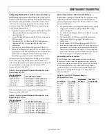
Configuring the PLL Band Select Value
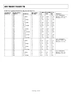
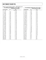
The PLL VCO has a valid operating range from approximately
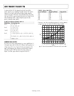
1.0 GHz to 2.0 GHz. This range is covered in 63 overlapping
frequency bands, as shown in Table 23. For any desired VCO
output frequency, there are multiple valid PLL band select values.
It is important to note that the data shown in Table 23 is for a
typical device. Device-to-device variations can shift the actual
VCO output frequency range by 30 MHz to 40 MHz. In addition,
the VCO output frequency varies as a function of temperature.
Therefore, it is required that the optimal PLL band select value
be determined for each individual device at a particular
operating temperature.
The device has an automatic PLL band select feature on chip.
When this feature is enabled, the device determines the optimal
PLL band setting for the device at the given temperature. This
setting holds for a ±60°C temperature swing in ambient tem-
perature. If the device is operated in an environment that
experiences a larger temperature swing, an offset should be
applied to the automatically selected PLL band.

