AD9776A/AD9778A/AD9779A
Rev. B | Page 42 of 56
DRIVING THE REFCLK INPUT
The REFCLK input requires a low jitter differential drive signal.
The signal level can range from 400 mV p-p differential to
1.6 V p-p differential centered about a 400 mV input common-
mode voltage. Looking at the single-ended inputs, or
REFCLK−, each input pin can safely swing from 200 mV p-p to
800 mV p-p about the 400 mV common-mode voltage. Although
these input levels are not directly LVDS compatible, REFCLK
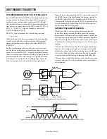
can be driven by an offset ac-coupled LVDS signal, as shown in
Figure 73.
LVDS_P_IN
50
Ω
50
Ω
0.1µF
0.1µF
LVDS_N_IN
REFCLK–
V
CM
= 400mV
0
645
2-
0
68
Figure 73. LVDS REFCLK Drive Circuit
If a clean sine clock is available, it can be transformer-coupled
to REFCLK, as shown in Figure 73. Use of a CMOS or TTL
clock is also acceptable for lower sample rates. It can be routed
through a CMOS to LVDS translator, and then ac-coupled as
described in this section. Alternatively, it can be transformer-
coupled and clamped, as shown in Figure 74.
50
Ω
50
Ω
TTL OR CMOS
CLK INPUT
REFCLK–
V
CM
= 400mV
BAV99ZXCT
HIGH SPEED
DUAL DIODE
0.1µF
06
452
-06
9
Figure 74. TTL or CMOS REFCLK Drive Circuit
A simple bias network for generating V
CM
is shown in Figure 75.
It is important to use CVDD18 and CGND for the clock bias
circuit. Any noise or other signal that is coupled onto the clock
is multiplied by the DAC digital input signal and can degrade
DAC performance.
0.1µF
1nF
1nF
V
CM
= 400mV
CVDD18
CGND
1k
Ω
287
Ω
06
45
2-
0
70
Figure 75. REFCLK V
CM
Generator Circuit

