AD9776A/AD9778A/AD9779A
Rev. B | Page 48 of 56
OPTIMIZING THE DATA INPUT TIMING
The AD9776A/AD9778A/AD9779A have on-chip circuitry that
enables the user to optimize the input data timing by adjusting
the relationship between the DATACLK output and DCLK_SMP
(the internal clock that samples the input data). This optimization
is made by a sequence of 3-wire interface register read and write
operations. The timing optimization can be done under strict
control of the user, or the device can be programmed to maintain a
configurable timing margin automatically. This function is only
available when the input data is referenced to the DATACLK
output. Each of these methods is detailed in the following section.
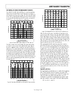
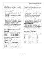
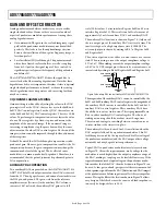
Figure 86 shows the circuitry that detects sample timing errors
and adjusts the data interface timing. The DCLK_SMP signal is
the internal clock used to latch the input data. Ultimately, it is
the rising edge of this signal that needs to be centered in the
valid sampling period of the input data. This is accomplished by
adjusting the time delay, t
D
, which changes the DATACLK
timing and, as a result, the arrival time of the input data with
respect to DCLK_SMP.
TIMING
ERROR IRQ
D
Q
Q
D
CLK
CLK
DCLK_SMP
PD1[0]
Δ
t
M
Δ
t
D
Δ
t
M
DATACLK
DELAY[3:0]
TIMING
MARGIN[3:0]
DATACLK
TIMING
ERROR TYPE
TIMING
ERROR
DETECTION
06
45
2-
4
02
Figure 86. Timing Error Detection and Optimization Circuitry
The error detect circuitry works by creating two sets of sampled
data (referred to as the margin test data) in addition to the
actual sampled data used in the device data path. One set of
sampled data is latched before the actual data sampling point.
The other set of sampled data is latched after the actual data
sampling point. If the margin test data match the actual data,
the sampling is considered valid and no error is declared. If
there is a mismatch between the actual data and the margin test
data, an error is declared.
The Data Timing Margin[3:0] variable determines how much
before and after the actual data sampling point the margin test
data are latched. Therefore, the data timing margin variable
determines how much setup and hold margin the interface
needs for the data timing error IRQ to remain inactive (show
error free operation). Therefore, the timing error IRQ is set
whenever the setup and hold margins drop below the Data
Timing Margin[3:0] value and does not necessarily indicate that
the data latched into the device is incorrect.
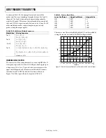
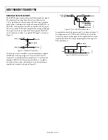
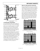
In addition to setting the data timing error IRQ, the data timing
error type bit is indicated when an error occurs. The data timing
error type bit is set low to indicate a hold error and high to
indicate a setup error. Figure 87 shows a timing diagram of the
data interface and the status of the data timing error type bit.
Δ
t
M
Δ
t
M
DATA
TIMING ERROR = 0
Δ
t
M
Δ
t
M
DATA
TIMING ERROR = 1
DATA TIMING ERROR TYPE = 1
Δ
t
M
Δ
t
M
DATA
DELAYED
DATA
SAMPLING
ACTUAL
SAMPLING
INSTANT
DELAYED
CLOCK
SAMPLING
TIMING ERROR = 1
DATA TIMING ERROR TYPE = 0
06
45
2-
4
03
Figure 87. Timing Diagram of Margin Test Data
Automatic Timing Optimization
When automatic timing optimization mode is enabled
(Register 0x03, Bit 7 = 1), the device continuously monitors
the data timing error IRQ and data timing error type bits. The
DATACLK Delay[3:0] is increased if a setup error is detected and
decreased if a hold error is detected. The value of the DATACLK
Delay[3:0] setting currently in use can be read back by the user.
Manual Timing Optimization
When the device is operating in manual timing optimization
mode (Register 0x03, Bit 7 = 0), the device does not alter the
DATACLK Delay[3:0] value from what is programmed by the
user. By default, the DATACLK delay enable bit is inactive. This
bit must be set high for the DATACLK Delay[3:0] value to be
realized. The delay (in absolute time) when programming
DATACLK delay between 00000 and 11111 varies from about
700 ps to about 6.5 ns. The typical delays per increment over
temperature are shown in Table 29.
Table 29. Data Delay Line Typical Delays Over Temperature
Delay
−40°C +25°C +85°C Unit
Zero Code Delay (Delay Upon
Enabling Delay Line)
630 700 740 ps
Average Unit Delay
175
190
210
ps
When the device is placed into manual mode, the error
checking logic is activated. If the IRQs are enabled, an interrupt
is generated if a setup/hold violation is detected. One error
check operation is performed per device configuration. Any
change to the Data Timing Margin[3:0] or DATACLK
Delay[3:0] values triggers a new error check operation.


