Rev.
PrD
Information furnished by Analog Devices is believed to be accurate and reliable.
However, no responsibility is assumed by Analog Devices for its use, nor for any
infringements of patents or other rights of third parties that may result from its use.
Specifications subject to change without notice. No license is granted by implication
or otherwise under any patent or patent rights of Analog Devices. Trademarks and
registered trademarks are the property of their respective owners.
One Technology Way, P.O. Box 9106, Norwood, MA 02062-9106, U.S.A.
Tel: 781.329.4700
www.analog.com
Fax: 781.326.8703
© 2005 Analog Devices, Inc. All rights reserved.
Dual 16-Bit, 1.0 GSPS
D/A Converter
Preliminary Technical Data
AD9779
FEATURES
•
1.8/3.3 V Single Supply Operation
•
Low power: 950mW (I
OUTFS
= 20 mA; f
DAC
= 1 GSPS, 4
×
Interpolation
•
DNL = ± 1.5 LSB, INL = ± 5.0 LSB
•
SFDR =82 dBc to f
OUT
= 100 MHz
•
ACLR = 87 dBc @ 80 MHz IF
•
CMOS data interface with Autotracking Input Timing
•
Analog Output: Adjustable 10-30mA (RL=25
Ω
to 50
Ω
)
•
100-lead Exposed Paddle TQFP Package
•
Multiple Chip Synchronization Interface
•
84dB Digital Interpolation Filter Stopband Attenuation
•
Digital Inverse Sinc Filter
APPLICATIONS
•
Wireless Infrastructure
Direct Conversion
Transmit Diversity
•
Wideband Communications Systems:
Point-to-Point Wireless, LMDS
PRODUCT DESCRIPTION
The AD9779 is a dual 16-bit high performance, high frequency
DAC that provides a sample rate of 1 GSPS, permitting multi
carrier generation up to its Nyquist frequency. It includes features
optimized for direct conversion transmit applications, including
complex digital modulation and gain and offset compensation. The
DAC outputs are optimized to interface seamlessly with analog
quadrature modulators such as the AD8349. A serial peripheral
interface (SPI) provides for programming many internal
parameters and also enables read-back of status registers. The
output current can be programmed over a range of 10mA to 30mA.
The AD9779 is manufactured on an advanced 0.18
µ
m CMOS
process and operates from 1.8V and 3.3V supplies for a total power
consumption of 950mW. It is supplied in a 100-lead QFP package.
PRODUCT HIGHLIGHTS
Ultra-low noise and Intermodulation Distortion (IMD) enable
high quality synthesis of wideband signals from baseband to high
intermediate frequencies.
Single-ended CMOS interface supports a maximum input rate of
300 MSPS with 1x interpolation.
Manufactured on a CMOS process, the AD9779 uses a proprietary
switching technique that enhances dynamic performance.
The current outputs of the AD9779 can be easily configured for
various single-ended or differential circuit topologies.
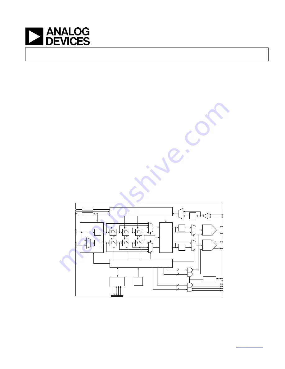
FUNCTIONAL BLOCK DIAGRAM
Complex
Modulator
Clock Generation/Distribution
2X
n * Fdac/8
n = 1, 2, 3… 7
P2D[15:0]
IOUT2_P
IOUT2_N
CLK+
CLK-
DATACLK_OUT
2X
2X
2X
2X
2X
Sinc
-1
Sinc
-1
16-Bit
IDAC
16-Bit
QDAC
Digital Controller
Clock
Multiplier
2X/4X/8X
Gain
Gain
Offset
Offset
Reference
& Bias
10
10
10
10
Power-On
Reset
Serial
Peripheral
Interface
Q Latch
I Latch
Delay Line
Delay Line
Data
Assembler
SDI
O
SD
O
SC
L
K
CSB
IOUT1_P
IOUT1_N
VREF
RSET
AUX1_P
AUX1_N
AUX2_P
AUX2_N
P1D[15:0]
SYNC_I
SYNC_O
Figure 1 Functional Block Diagram


