Preliminary Technical Data
AD9779
Rev. PrD | Page 17 of 34
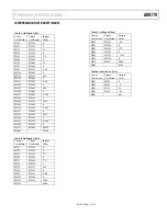
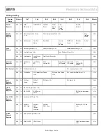
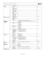
7 Data
Delay
Error
(read only)
0
6 Chip
Synchronization
Delay Error (read
only)
0
5 Cross
Control
Error (read only)
0
3 Data
Delay
Error
Enable
0
2 Chip
Synchronization
Error Enable
0
06
IRQ Status
1 Cross
Control
Error Enable
0
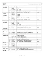
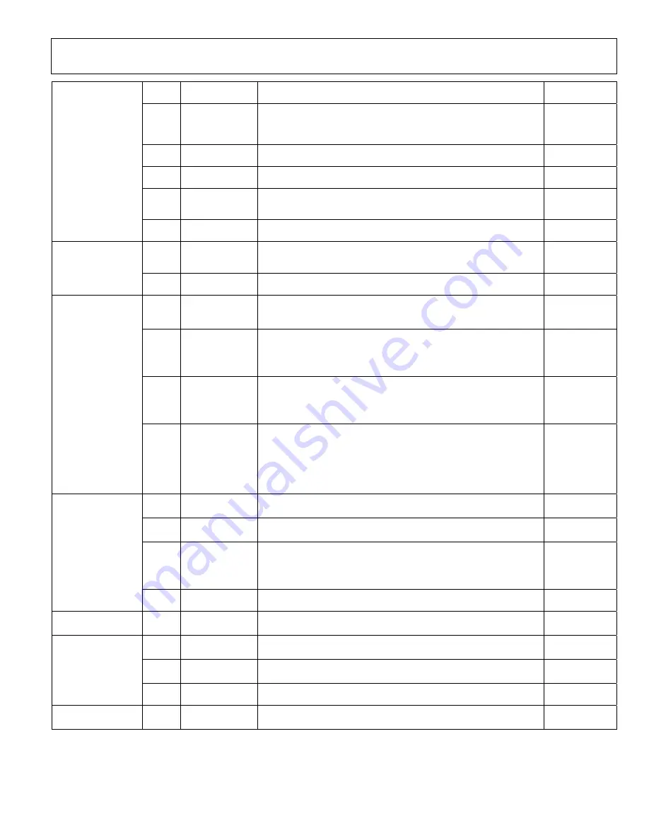
7:3
PLL Band Select
See
Table 14
for
values.
11001
07
PLL Band and Divide
2:0
PLL Ripple Cap
Adjust
111
7
PLL Enable
0: PLL off, DAC rate clock supplied by outside source
1: PLL on, DAC rate clock synthesized internally from data rate clock via PLL
clock multiplier
0
6:5
PLL Output Divide
Ratio
00: Divide by 1
01: Divide by 2
10: Divide by 4
11: Divide by 8
01
4:3 PLL
Loop
Feedback Divide
Ratio
00: Divide by 1
01: Divide by 2
10: Divide by 4
11: Divide by 8
10
08
PLL Enable and
Charge Pump
Control
2:0
PLL Loop Filter
Bandwidth Tuning
Recommended
Settings. See
Table 14
for PLL
Band Select
values.
000: PLL band select 00000-00111
100: PLL band select 01000-01111
110: PLL band select 10000-10111
111: PLL band select 11000-11111
111
7
PLL Error Bit
Source
0: Phase error detect
1: Range limit
0
6 PLL
Reference
Bypass
0: Use PLL reference
1: Use DAC reference
0
5:3
VCO AGC Gain
Control. See
Table
14
for PLL Band
Select values.
000: PLL band select 00000-00111
100: PLL band select 01000-01111
110: PLL band select 10000-10111
111: PLL band select 11000-11111
111
09
Misc. Control
2:0
PLL Bias Current
Level/Trim
000
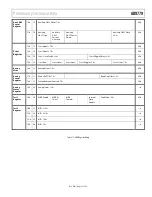
0A
IDAC Gain
7:0 IDAC
Gain
Adjustment
(7:0) LSB slice of 10 bit gain setting word for IDAC
11111001
7
IDAC Sleep
0: IDAC on
1: IDAC off
0
6
IDAC Power Down
0: IDAC on
1: IDAC off
0
0B
IDAC Gain and
Control
1:0 IDAC
Gain
Adjustment
(9:8) MSB slice of 10 bit gain setting word for IDAC
01
0C
Auxiliary DAC1 Gain
7:0 Aux
DAC1
Gain
Adjustment
(7:0) LSB slice of 10 bit gain setting word for Aux DAC1
00000000


