Preliminary Technical Data
AD9779
Rev. PrD | Page 23 of 34
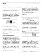
The power down bit (register 00h, bit 4) controls the power down
function for the digital section of the AD9779. The power down
function in bit 4 works in conjunction with TxEnable (pin 39)
according to the following;
TxEnable =
0:PWDWN=
0: Flush data path with zeroes
1: Digital engine in power down state, DACs and
reference are not affected.
1: Normal operation
Internal PLL Clock Multiplier / Clock Distribution
The internal clock structure on the AD9779 allows the user to drive
the differential clock inputs with a clock at 1x or an integer multiple
of the input data rate, or at the DAC output sample rate. A PLL
internal to the AD9779 provides input clock multiplication and
provides all of the internal clocks required for the interpolation
filters and data synchronization.
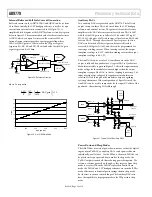
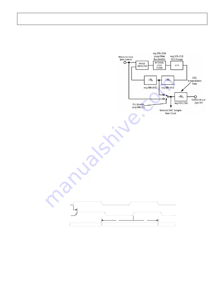
The internal clock architecture is shown in Figure 32. The
reference clock is the differential clock at pins 5 and 6. This clock
input can be run differentially, or singled ended by driving pin 5
with a clock signal, and biasing pin 6 to the mid swing point of the
signal at pin 5. There are various configurations in which this clock
architecture can be run;
1.
PLL Enabled (reg 08h, bit 7=1) – The PLL enable switch
in Figure 32 is connected to the junction of the dividers
N1 and N2. Divider N3 determines the interpolation rate
of the DAC, and the ratio N2/N3 determines the ratio of
Reference Clock/Input Data Rate. The VCO runs
optimally over the range 804MHz to 1800MHz, so that
N1 is used to keep the speed of the VCO in this range,
even though the DAC sample rate may be lower. The loop
filter components are entirely internal and no external
compensation is necessary.
2.
PLL Disabled (reg 08h, bit 7=0) – The PLL enable switch
in Figure 32 is connected to the Reference Clock Input.
The differential reference clock input will be the DAC
output sample rate and N3 will determine the
interpolation rate.
Figure 32. Internal Clock Architecture of AD9779
Timing Information
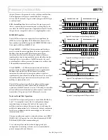
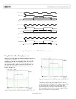
Figure 33 through Figure 35 show some of the various timing
possibilities when the PLL is enabled. The combination of the
settings of N2 and N3 means that the reference clock frequency
may be a multiple of the actual input data rate. Figure 33 through
Figure 35 show, respectively, what the timing looks like when
N2/N3 = 1, 2, and 4.
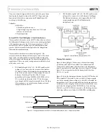
Figure 36 shows the timing specifications for the AD9779 when the
PLL is disabled. The reference clock is at the DAC output sample
rate. In the example shown in Figure 36, if the PLL is disabled, the
interpolation is 4x.. The set up and hold time for the input data are
with respect to the rising edge of the reference clock which occurs
just before the rising edge of the DATACLK out. Note that if reg
02h, bit2 is set, DATACLK out is inverted so the latching reference
clock edge will occur just before the DATACLK out falling edge.
tH
tS
tD
Refe rence Clock
DATA CLK out
Input Data
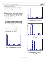
Figure 33. Timing Specifications for AD9779, PLL Enabled, Reference Clock = 1x Input Sample Rate

