ADM1060
Rev. B | Page 15 of 52
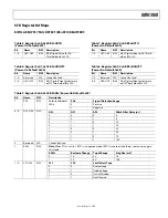
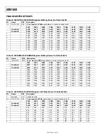
SFD Register Bit Maps
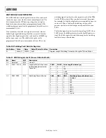
BIPOLAR SUPPLY FAIL DETECT (BSn SFD) REGISTERS
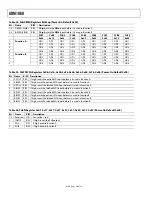
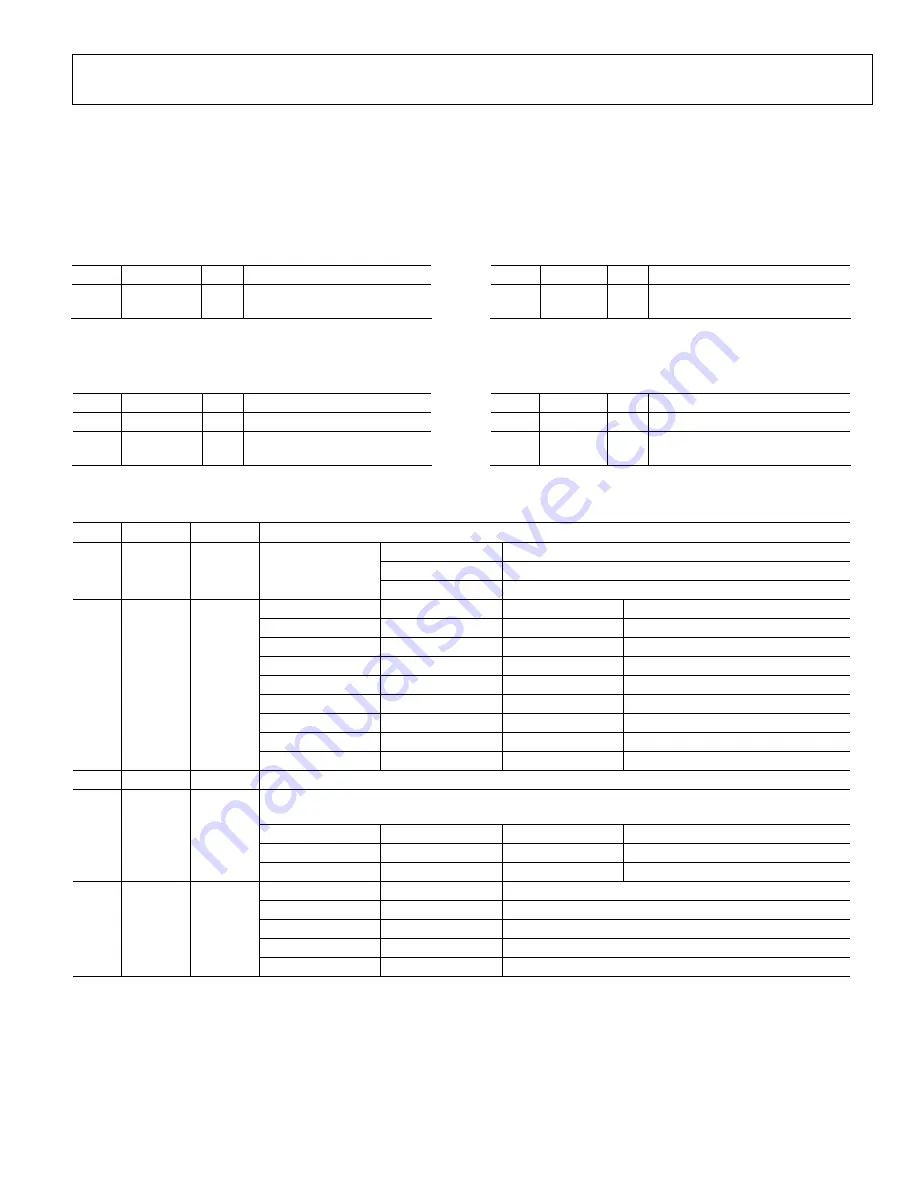
Table 5. Register 0xA0, 0xA8 BSnOVTH
(Power-On Default 0xFF)
Bit Name R/W
Description
7–0 OV7–OV0 R/W
8-Bit Digital Value for OV
Threshold on BSn SFD
Table 6. Register 0xA1, 0xA9 BSnOVHYST
(Power-On Default 0x00)
Bit Name
R/W
Description
7–5
Reserved
N/A
Cannot Be Used
4–0 HY4–HY0 R/W
5-Bit Digital Value for Hysteresis
on OV Threshold of BSn SFD
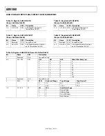
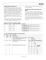
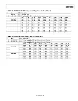
Table 7. Register 0xA2, 0xAA BSnUVTH
(Power-On Default 0x00)
Bit Name R/W
Description
7–0
UV7–UV0
R/W
8-Bit Digital Value for UV Thresh-
old on BSn SFD
Table 8. Register 0xA3, 0xAB BSnUVHYST
(Power-On Default 0x00)
Bit Name R/W
Description
7–5
Reserved
N/A
Cannot Be Used
4–0
HY4–HY0
R/W
5-Bit Digital Value for Hysteresis
on UV Threshold of BSn SFD
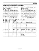
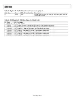
Table 9. Register 0xA4, 0xAC BSnSEL (Power-On Default 0x00)
Bit Name R/W
Description
POL
Sign of Detection Range
0 Positive
7 POL R/W Polarity of Bipolar
SFDn
1 Negative
GF2 GF1 GF0 Glitch
Filter
Delay
(µs)
0 0 0 0
0 0 1 5
0 1 0 10
0 1 1 20
1 0 0 30
1 0 1 50
1 1 0 75
6−4 GF2−GF0
R/W
1 1 1 100
3
Reserved
N/A
Cannot Be Used
Note:
When POL is set to 1 (SFD is in negative mode), RSEL is unused since there is only one range in
this mode.
RSEL1
Bottom of Range
Top of Range
Step Size (mV)
0
1 V
3 V
7.8
2 RSEL R/W
1
2 V
6 V
15.6
FS1
FS0
Fault Select Type
0 0 Overvoltage
0 1 Undervoltage
1 0 Out-of-Window
1−0 FS1−FS0 R/W
1 1 Not
Allowed


