ADM1060
Rev. B | Page 19 of 52
GENERAL-PURPOSE INPUTS (GPIs)
The ADM1060 has four general-purpose logic inputs (GPIs).
These are TTL/CMOS logic level compatible. Standard logic
signals can be applied to the pins: RESET from reset generators,
PWRGOOD signals, fault flags, manual resets, and so on. These
signals can be gated with the other inputs supervised by the
ADM1060 and used to control the status of the PDOs. The
inputs can be simply buffered, or a logic transition can be
detected and a pulse output generated. The width of this pulse is
programmable from 10 µs to a maximum of 10 ms. The
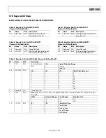
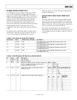
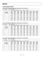
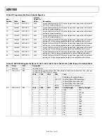
configuration of the GPIs is shown in the register and bit maps
below.
The GPIs also feature a glitch filter similar to that provided on
the SFDs. This enables the user to ignore spurious transitions
on the GPIs. For example, the glitch filter can be used to
debounce a manual reset switch. The length of the glitch filter
can also be programmed.
LOGIC STATE OF THE GPIs AND OTHER LOGIC
INPUTS
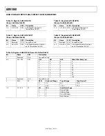
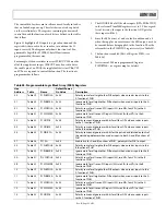
Each of the GPIs can have a weak (10 µA) pull-down current
source. The current sources can be connected to the inputs by
progamming the relevant bit in the PDEN register. This enables
the user to control the condition of these inputs, pulling them to
GND even when they are unused or left floating.
Note that the same pull-down function is provided for the
SMBus address pins, A0 and A1, and for the WDI pin. A register
is used to program which of the inputs is connected to the cur-
rent sources.
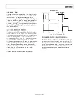
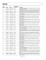
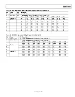
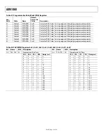
Table 22. General-Purpose Inputs (GPIn) Registers
Hex Address
Name
Default Power-On Value
Description
98 GPI4CFG
0x00
GPI4 configuration setup of the glitch filter delay, pulse width,
level/edge detection, etc.
99 GPI3CFG
0x00
GPI3 configuration setup of the glitch filter delay, pulse width,
level/edge detection, etc.
9A GPI2CFG
0x00
GPI2 configuration setup of the glitch filter delay, pulse width,
level/edge detection, etc.
9B GPI1CFG
0x00
GPI1 configuration setup of the glitch filter delay, pulse width,
level/edge detection, etc.
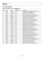
Table 23. GPInCFG Registers Bit Map (Power-On Default 0x00)
Bit Name R/W Description
7
Reserved
N/A
Cannot Be Used
6
INVIN
R/W
If High, Invert Input
INTYP Detect
0 Detect
Level
5 INTYP R/W
Determines whether a Level or an Edge is Detected on
the Pin. If an edge is detected, a positive pulse of
programmable length is output.
1
Detect Edge
PULS1
PULS0
Pulse Length Selected (µs)
0 0 10
0 1 100
1 0 1,000
4–3 PULS1−0
R/W Length of Pulse Output Once an Edge Has Been
Detected on Input
1 1 10,000
GF2 GF1 GF0
Glitch Filter
Delay (µs)
0 0 0 0
0 0 1 5
0 1 0 10
0 1 1 20
1 0 0 30
1 0 1 50
1 1 0 75
2–0
GF2−GF0
R/W
Length of Time for which the Input Is Ignored
1 1 1 100

