ADM1060
Rev. B | Page 23 of 52
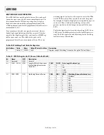
The control bits for these macrocells are stored locally in latches
that are loaded at power-up. These latches can also be updated
via the serial interface. The registers containing the macrocell
control bits and the function of each bit are defined in the tables
that follow.
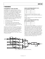
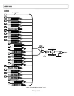
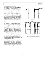
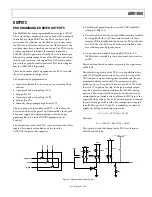
Figure 21 highlights all 21 inputs to a given function and the
register/bits that need to be set in order to condition the 21
inputs correctly. The diagram only shows function A of Pro-
grammable Logic Block 1 (PLB1), but all functions are
programmed in the same way.
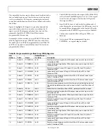
For example, if the user wishes to assert PLBOUT 200 ms after
all of the supplies are in spec (PLBOUT may be used to drive
the enable pin of an LDO), the supply fault detectors VBn, VH,
and VPn are required to control the function. The function is
programmed as follows:
1.
The IGNORE bit of all the other inputs (GPIs, PDBs, WDI)
in the relevant P1xxxIMK registers is set to 1. Thus, regard-
less of its status, the input to the function AND gate for
these inputs will be 1.
2.
Since the SFDs assert a 1 under a fault condition and a 0
when the supplies are in tolerance, the SFD outputs need to
be inverted before being applied to the function. Thus the
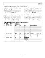
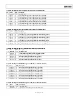
relevant bit in the P1SFDPOL register is set (see Table 38).
3.
The function is enabled (
B
it 1 of
R
egister P1EN—see
4.
A rise time of 200 ms is programmed (register
P1PDBTIM—see register map for details).
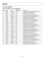
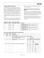
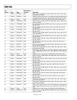
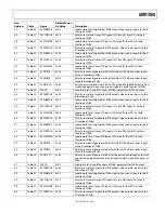
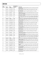
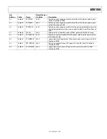
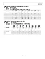
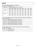
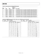
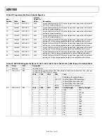
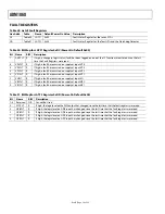
Table 28. Programmable Logic Block Array (PLBA) Registers
Hex
Address Table
Name
Default Power-
On Value
Description
P1PLBPOLA
0x00
Polarity sense for all eight other PLB outputs when used as inputs to the
A function of PLB1
P1PLBIMKA
0x00
Ignore mask for all eight other PLB outputs when used as inputs to the A
function of PLB1
P1SFDPOLA
0x00
Polarity sense for all seven SFD inputs (VH, two VBs, four VPs) to the A
function of PLB1
P1SFDIMKA
0x00
Ignore mask for all seven SFD inputs (VH, two VBs, four VPs) to the A
function of PLB1
P1GPIPOL
0x00
Polarity sense and ignore mask bits for all four GPIs when used as inputs
to the A function of PLB1
P1GPIIMK
0x00
Polarity sense and ignore mask bits for all four GPIs when used as inputs
to the B function of PLB1
P1WDICFG
0x00
Polarity sense and ignore mask bits for the pulsed and latched outputs of
the watchdog detector when used as inputs to both A and B functions of
PLB1
07
PS1EN
0x00
Enable bits for A and B functions of PLB1, polarity bit for PLB1 output
P1PLBPOLB
0x00
Polarity sense for all eight other PLB outputs when used as inputs to the
B function of PLB1
P1PLBIMKB
0x00
Ignore mask for all eight other PLB outputs when used as inputs to the B
function of PLB1
P1SFDPOLB
0x00
Polarity sense for all seven SFD inputs (VH, two VBs, four VPs) to the B
function of PLB1
P1SFDIMKB
0x00
Ignore mask for all seven SFD inputs (VH, two VBs, four VPs) to the B
function of PLB1
P2PLBPOLA
0x00
Polarity sense for all eight other PLB outputs when used as inputs to the
A function of PLB2
P2PLBIMKA
0x00
Ignore mask for all eight other PLB outputs when used as inputs to the A
function of PLB2
P2SFDPOLA
0x00
Polarity sense for all seven SFD inputs (VH, two VBs, four VPs) to the A
function of PLB2
P2SFDIMKA
0x00
Ignore mask for all seven SFD inputs (VH, two VBs, four VPs) to the A
function of PLB2
P2GPIPOL
0x00
Polarity sense and ignore mask bits for all four GPIs when used as inputs
to the A function of PLB2

