ADM1060
Rev. B | Page 31 of 52
PROGRAMMABLE DELAY BLOCK
Each output of the PLBA is fed into a separate programmable
delay block (PDB). The PDB enables the user to add a delay to
the logic block output before it is applied to either a PDO or one
of the other PLBs (the output of a PLB can be the input to any
of the other PLBs, but not itself). The PDB operation is similar
to that of the glitch filter (discussed in the SFD section). There
is an important difference between the two functions, however.
The delay on the falling edge of an input to the PDB can be
programmed independently of the rising edge. This allows the
user to program the length of the pulse output from the PDB.
Thus, for instance, the width of the pulse from the watchdog
fault detector can be adjusted, or the user can ensure that a sup-
ply supervised by one of the SFDs is within its UV/OV range
for a programmed period of time before asserting a PDO. A
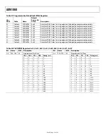
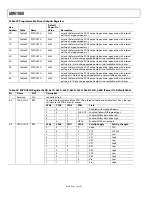
delay of 0 ms to 500 ms can be programmed in the PnPDBTIM
registers. Four bits each are used to program the rising edge and
falling edge.
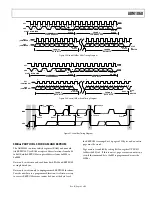
Once programmed, the PDB operates as follows. If the user
programs a delay on the rising edge of, say, 200 ms, the PDB
looks for a rising edge on the input. Once it sees the edge it
starts a timer. If the input remains high and the timer reaches
200 ms, the PDB immediately outputs a rising edge. If the input
falls low before the timer has reached 200 ms, no edge is output
from the PDB and the timer is reset. Because there is separate
control over the falling edge, if no delay is programmed on the
falling edge, the delay defaults to 0 ms and a falling edge on the
input will immediately appear on the output. If a falling edge
delay is programmed, the PDB operates exactly the opposite as
it does for a rising edge. Again, if a delay of, say, 200 ms is pro-
grammed on the falling edge, the PDB looks for a falling edge
on the input. Once it sees the edge, it starts a timer. If the input
remains low and the timer reaches 200 ms, the output transi-
tions from high to low. A valid rising edge must appear at the
output before a falling edge delay can be activated. The function
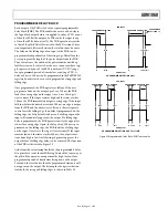
of the PDB is illustrated in Figure 22.
Aside from the extra timing flexibility, the programmable delay
also provides a crude form of filtering. In much the same way as
the glitch filter operates, an input must be high (or low) for a
programmed period of time before being seen on the output.
Transients that are shorter than the programmed timeouts will
not appear on the output. The bit map for the register that con-
trols both the rising and falling edges is shown in Table 38.
PROGRAMMED RISE TIME
PROGRAMMED RISE TIME
PROGRAMMED
FALL TIME = 0
t
0
t
RISE
t
0
t
RISE
t
FALL
t
0
t
RISE
t
0
t
RISE
t
FALL
PDB INPUT
PDB OUTPUT
PROGRAMMING RISE TIME ONLY
PDB INPUT
t
0
t
RISE
t
1
t
FALL
t
0
t
RISE
t
1
t
FALL
t
0
t
RISE
t
1
t
FALL
t
0
t
RISE
t
1
t
FALL
PDB OUTPUT
PROGRAMMING RISE TIME AND FALL TIME
PROGRAMMED
RISE TIME
PROGRAMMED
FALL TIME
PROGRAMMED
RISE TIME
PROGRAMMED
FALL TIME
Figure 22. Programmable Delay Block (PDB) Functionality

