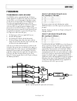
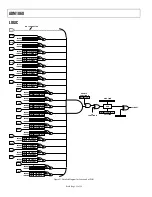
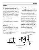
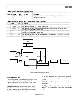
background image

ADM1060 


Rev. B | Page 32 of 52 

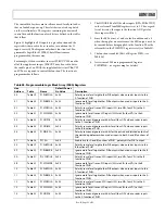
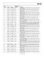
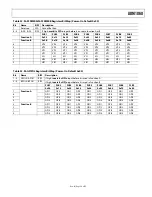
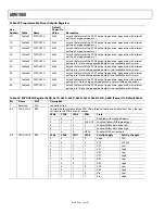
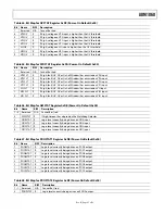
Table 37. Programmable Delay Block (PDB) Registers 

Hex 
Addr. Table  Name 

Default 
Power-On 
Value Description 


0C 

Table 38 

P1PDBTIM 

0x00 

Delay for PDB1. Delay for rising edge and falling edge programmed separately.  

1C 

Table 38 

P2PDBTIM 

0x00 

Delay for PDB2. Delay for rising edge and falling edge programmed separately.  

2C 

Table 38 

P3PDBTIM 

0x00 

Delay for PDB3. Delay for rising edge and falling edge programmed separately.  

3C 

Table 38 

P4PDBTIM 

0x00 

Delay for PDB4. Delay for rising edge and falling edge programmed separately.  

4C 

Table 38 

P5PDBTIM 

0x00 

Delay for PDB5. Delay for rising edge and falling edge programmed separately.  

5C 

Table 38 

P6PDBTIM 

0x00 

Delay for PDB6. Delay for rising edge and falling edge programmed separately.  

6C 

Table 38 

P7PDBTIM 

0x00 

Delay for PDB7. Delay for rising edge and falling edge programmed separately.  

7C 

Table 38 

P8PDBTIM 

0x00 

Delay for PDB8. Delay for rising edge and falling edge programmed separately.  

8C 

Table 38 

P9PDBTIM 

0x00 

Delay for PDB9. Delay for rising edge and falling edge programmed separately.  


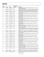
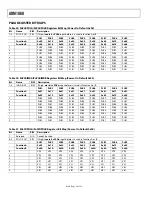
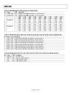
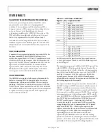
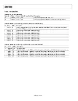
Table 38. PnPDBTIM Registers 0x0C, 0x1C, 0x2C, 0x3C, 0x4C, 0x5C, 0x6C, 0x7C, 0x8C 

Bit Name  R/W Description 

Bit Name  R/W Description 

7–4 

TR3−TR0 

Programmed Rise Time 

3–0 

TF3−TF0 

Programmed Fall Time  

TR3 TR2 TR1 TR0 Delay 

(ms) 

TF3 TF2 TF1 TF0 Delay 

(ms) 

0 0 0 0 0 

0 0 0 0 0 

0 0 0 1 1 

0 0 0 1 1 

0 0 1 0 2 

0 0 1 0 2 

0 0 1 1 5 

0 0 1 1 5 

0 1 0 0 10 

0 1 0 0 10 

0 1 0 1 20 

0 1 0 1 20 

0 1 1 0 40 

0 1 1 0 40 

0 1 1 1 60 

0 1 1 1 60 

1 0 0 0 80 

1 0 0 0 80 

1 0 0 1 100 

1 0 0 1 100 

1 0 1 0 150 

1 0 1 0 150 

1 0 1 1 200 

1 0 1 1 200 

1 1 0 0 250 

1 1 0 0 250 

1 1 0 1 300 

1 1 0 1 300 

1 1 1 0 400 

1 1 1 0 400 


1 1 1 1 500 


1 1 1 1 500 


Summary of Contents for ADM1060

Page 1: ...ervoltage or out of window undervoltage or overvoltage conditions The inputs to these supply fault detectors are via the VH high voltage pin VBn positive or negative pins and VPn positive only pins Either the VH supply or one of the VPn supplies is used to power the ADM1060 whichever is highest This ensures that in the event of a supply failure the ADM1060 is kept alive for as long as possible thu...

Page 2: ...Data sheet changed from Rev A to Rev B Changes to Specifications 5 Changes to Outputs section 33 Updated Outline Dimensions 50 5 03 Data sheet changed from Rev 0 to Rev A Changes to Features 1 Changes to Specifications 5 Changes to Figure 1 4 Changes to Absolute Maximum Ratings 7 Changes to Figures 2 8 15 16 8 10 Changes to Figure 17 11 Changes to Programmable Supply Fault Detectors section 11 Cha...

Page 3: ...will not assert until the VP2 VP3 and VP4 supplies are in tolerance VB1 and VH have been in tolerance for 200 ms and PDO7 has already been asserted A simple sequencing operation would be to daisy chain each PLB output into the input of the next PLB such that PDO9 does not assert until PDO8 asserts which in turn does not assert until PDO7 asserts and so on All of the functional capability described...

Page 4: ... PLB MACROCELL 8 PLB MACROCELL 9 PROGRAMMABLE LOGIC BLOCK ARRAY PLBA HIGH SUPPLY 14 4V FAULT DETECTOR POSITIVE SUPPLY FAULT DETECTOR 1 POSITIVE SUPPLY FAULT DETECTOR 4 BIPOLAR SUPPLY FAULT DETECTOR 1 BIPOLAR SUPPLY FAULT DETECTOR 2 INPUT LOGIC SIGNAL CONDITION WATCHDOG FAULT DETECTOR VREF ADM1060 INTERNAL 5 25V SUPPLY REGULATED 5 25V SUPPLY CHARGE PUMP VDD ARBITRATOR SMBus INTERFACE DEVICE CONTROL...

Page 5: ...Ω From VBn to GND negative mode Absolute Accuracy VH VPn VBn Inputs 2 5 2 5 Calibrated Absolute Accuracy3 VH VPn Inputs 1 0 1 0 Factory preprogrammed to specific thresholds VBn Inputs 1 5 1 5 Factory preprogrammed to specific thresholds Glitch Filters Digital 0 100 µs See Figure 19 Eight timeout options between 0 µs and 100 µs PROGRAMMABLE DRIVER OUTPUTS High Voltage Charge Pump Mode PDOs 1 to 4 O...

Page 6: ...Time tLOW 4 7 µs See Figure 27 SCL High Time tHIGH 4 µs See Figure 27 SCL SDA Rise Time tr 1000 ns See Figure 27 SCL SDA Fall Time tf 300 µs See Figure 27 Data Setup Time tSU DAT 250 ns See Figure 27 Data Hold Time tHD DAT 300 ns See Figure 27 NOTES 1 At least one VPn must be 3 0 V if used as supply VH must be 4 5 V if used as supply 2 Specification is not production tested but is supported by cha...

Page 7: ...ture Range 65 C to 150 C Lead Temperature Soldering Vapor Phase 60 sec 215 C ESD Rating All Pins 2000 V Stresses above those listed under Absolute Maximum Ratings may cause permanent damage to the device This is a stress rat ing only functional operation of the device at these or any other conditions above those indicated in the operational sec tion of this specification is not implied Exposure to...

Page 8: ... 5 1 0 0 5 0 0 1 2 3 5 4 Figure 3 IDD vs VVP1 Supply VVP1 V I VP1 µA 300 250 200 150 100 50 0 0 1 3 2 4 5 Figure 4 IVP1 vs VVP1 Not Supply VVH V I DD mA 4 0 3 0 2 0 0 0 2 4 6 10 8 12 14 16 0 5 1 0 2 5 1 5 3 5 Figure 5 IDD vs VVH VVH V I VH µA 250 200 150 100 50 0 0 1 2 3 4 6 5 Figure 6 IVH vs VVH Not Supply VVB1 V I VB1 µA 300 200 100 0 100 200 300 400 6 4 2 0 4 6 2 Figure 7 IVB1 vs VVB1 ...

Page 9: ...s Temperature ILOAD mA V PDO V 3 0 3 5 4 0 4 5 2 5 2 0 1 5 1 0 0 5 0 0 0 5 1 0 1 5 2 VVP1 3 3V VVP1 5V Figure 10 VPDO Strong Pull Up to VP1 vs Load Current ILOAD µA V PDO V 4 5 4 0 3 5 3 0 2 5 2 0 1 5 1 0 0 5 0 0 5 10 15 20 25 30 40 35 VVP1 5V VVP1 3 3V Figure 11 VPDO Weak Pull Up to VP1 vs Load Current ILOAD mA V PDO V 1 00 0 75 0 50 0 25 0 0 2 4 6 10 8 Figure 12 VPDO Strong Pull Down vs Load Cur...

Page 10: ...5 80 Figure 14 Oscillator Frequency vs Temperature ILOAD µA VCCP V 6 00 5 75 5 50 5 25 5 00 4 75 4 50 0 100 200 300 500 400 VVDDCAP 2 7V VVDDCAP 4 75V Figure 15 VCCP vs Load Current TEMPERATURE C GPI THRESHOLD V 3 0 2 5 2 0 1 5 1 0 0 5 0 40 25 10 5 20 35 50 65 80 VVDDCAP 2 7V VVDDCAP 4 75V Figure 16 GPI Threshold vs Temperature ...

Page 11: ...le if VP1 is connected to a 3 3 V supply VDD will power up to approximately 3 1 V through VP1 If VP2 is then connected to another 3 3 V supply VP1 will still power the device unless VP2 goes 100 mV higher than VP1 A second capacitor is required on the VCCP pin of the ADM1060 This capacitor is the reservoir capacitor for the central charge pump Again a 1 µF capacitor is recommended for this functio...

Page 12: ...grammable Supply Fault Detector SFD COMPARATOR HYSTERESIS The OV and UV comparators shown in Figure 18 are always looking at VPn via a potential divider In order to avoid chattering multiple transitions when the input is very close to the set threshold level these comparators have digitally programmable hysteresis The UV and OV hysteresis can be programmed in two registers that are similar but sep...

Page 13: ...able hysteresis of the SFDs The glitch filter timeout is programmable up to 100 µs If a pulse shorter than the programmed timeout appears on the input this pulse is masked and the signal change will appear on the output If an input pulse longer than the programmed timeout appears on the input this pulse will appear on the output The output will be delayed with respect to the input by the length of...

Page 14: ...PS1OVTH 0xFF Overvoltage Threshold for Positive Voltage SFD1 PS1SFD B9 Table 16 PS1OVHYST 0x00 Digital Hysteresis on OV Threshold for PS1SFD BA Table 17 PS1UVTH 0x00 Undervoltage Threshold for PS1SFD BB Table 18 PS1UVHYST 0x00 Digital Hysteresis on UV Threshold for PS1SFD BC Table 19 PS1SEL 0x00 Glitch Filter Range and Fault Type Select for PS1SFD C0 Table 15 PS2OVTH 0xFF Overvoltage Threshold for...

Page 15: ... 0xA3 0xAB BSnUVHYST Power On Default 0x00 Bit Name R W Description 7 5 Reserved N A Cannot Be Used 4 0 HY4 HY0 R W 5 Bit Digital Value for Hysteresis on UV Threshold of BSn SFD Table 9 Register 0xA4 0xAC BSnSEL Power On Default 0x00 Bit Name R W Description POL Sign of Detection Range 0 Positive 7 POL R W Polarity of Bipolar SFDn 1 Negative GF2 GF1 GF0 Glitch Filter Delay µs 0 0 0 0 0 0 1 5 0 1 0...

Page 16: ... R W 8 Bit Digital Value for UV Threshold on HV SFD Table 13 Register 0xB3 HSUVHYST Power On Default 0x00 Bit Name R W Description 7 5 Reserved N A Cannot Be Used 4 0 HY4 HY0 R W 5 Bit Digital Value for Hysteresis on UV Threshold of HV SFD Table 14 Register 0xB4 HSSEL Power On Default 0x00 Bit Name R W Description 7 Reserved N A Cannot Be Used GF2 GF1 GF0 Glitch Filter Delay µs 0 0 0 0 0 0 1 5 0 1...

Page 17: ...UV7 UV0 R W 8 Bit Digital Value for UV Thresh old on PSn SFD Table 18 Register 0xBB 0xC3 0xCB 0xD3 PSnUVHYST Power On Default 0x00 Bit Name W Description 7 5 Reserved N A Cannot Be Used 4 0 HY4 HY0 R W 5 Bit Digital Value for Hysteresis on UV Threshold of PSn SFD Table 19 Register 0xBC 0xC4 0xCC 0xD4 PSnSEL Power On Default 0x00 Bit Name R W Description 7 Reserved N A Cannot Be Used GF2 GF1 GF0 Gl...

Page 18: ...high low high pulse were required by a proces sor to reset Thus a fault on the watchdog can be used to generate a pulsed or latched output on any or all of the nine PDOs The latched signal can be cleared low by reading LATF1 then LATF2 across the SMBus interface see the Fault Registers sec tion The RAM register list and the bit map for the watchdog fault detector are shown below Table 20 Watchdog ...

Page 19: ... GND even when they are unused or left floating Note that the same pull down function is provided for the SMBus address pins A0 and A1 and for the WDI pin A register is used to program which of the inputs is connected to the cur rent sources Table 22 General Purpose Inputs GPIn Registers Hex Address Name Default Power On Value Description 98 GPI4CFG 0x00 GPI4 configuration setup of the glitch filt...

Page 20: ...igh address pin A1 is pulled to GND using a 10 µA pull down current source 5 PDENA0 R W If high address pin A0 is pulled to GND using a 10 µA pull down current source 4 PDENWDI R W If high WDI is pulled to GND using a 10 µA pull down current source 3 PDENGPI4 R W If high GPI4 is pulled to GND using a 10 µA pull down current source 2 PDENGPI3 R W If high GPI3 is pulled to GND using a 10 µA pull dow...

Page 21: ...ND gate The effect of setting these bits can be seen in Figure 20 The inverting gate shown is an XOR gate resulting in the following truth table Table 26 Truth Table for PLB Input Inversion POL Input Signal XOR Output 0 0 0 0 1 1 1 0 1 1 1 0 The last two entries in the truth table show that with the INVERT POL bit set the XOR output is always the inverse of the input Similarly the ignore gate show...

Page 22: ...B2 0x02 P1SFDPOLA 2 0x03 P1SFDIMKA 2 INVERT IGNORE VH 0x02 P1SFDPOLA 3 0x03 P1SFDIMKA 3 INVERT IGNORE VP1 0x02 P1SFDPOLA 4 0x03 P1SFDIMKA 4 INVERT IGNORE VP2 0x02 P1SFDPOLA 5 0x03 P1SFDIMKA 5 INVERT IGNORE VP3 0x02 P1SFDPOLA 6 0x03 P1SFDIMKA 6 INVERT IGNORE VP4 0x04 P1GPIPOL 4 0x05 P1GPIIMK 4 INVERT IGNORE GPI1 0x04 P1GPIPOL 5 0x05 P1GPIIMK 5 INVERT IGNORE GPI2 0x04 P1GPIPOL 6 0x05 P1GPIIMK 6 INVE...

Page 23: ...mask for all eight other PLB outputs when used as inputs to the A function of PLB1 02 Table 31 P1SFDPOLA 0x00 Polarity sense for all seven SFD inputs VH two VBs four VPs to the A function of PLB1 03 Table 32 P1SFDIMKA 0x00 Ignore mask for all seven SFD inputs VH two VBs four VPs to the A function of PLB1 04 Table 33 P1GPIPOL 0x00 Polarity sense and ignore mask bits for all four GPIs when used as i...

Page 24: ...ion of PLB3 26 Table 35 P3WDICFG 0x00 Polarity sense and ignore mask bits for the pulsed and latched outputs of the watchdog detector when used as inputs to both A and B functions of PLB3 27 Table 36 PS3EN 0x00 Enable bits for A and B functions of PLB3 polarity bit for PLB3 output 28 Table 29 P3PLBPOLB 0x00 Polarity sense for all eight other PLB outputs when used as inputs to the B function of PLB...

Page 25: ...puts to the B function of PLB5 4A Table 31 P5SFDPOLB 0x00 Polarity sense for all seven SFD inputs VH two VBs four VPs to the B function of PLB5 4B Table 32 P5SFDIMKB 0x00 Ignore mask for all seven SFD inputs VH two VBs four VPs to the B function of PLB5 50 Table 29 P6PLBPOLA 0x00 Polarity sense for all eight other PLB outputs when used as inputs to the A function of PLB6 51 Table 30 P6PLBIMKA 0x00...

Page 26: ...00 Ignore mask for all eight other PLB outputs when used as inputs to the A function of PLB8 72 Table 31 P8SFDPOLA 0x00 Polarity sense for all seven SFD inputs VH two VBs four VPs to the A function of PLB8 73 Table 32 P8SFDIMKA 0x00 Ignore mask for all seven SFD inputs VH two VBs four VPs to the A function of PLB8 74 Table 33 P8GPIPOL 0x00 Polarity sense and ignore mask bits for all four GPIs when...

Page 27: ...s of the watchdog detector when used as inputs to both A and B functions of PLB9 87 Table 36 PS9EN 0x00 Enable bits for A and B functions of PLB9 polarity bit for PLB9 output 88 Table 29 P9PLBPOLB 0x00 Polarity sense for all eight other PLB outputs when used as inputs to the B function of PLB9 89 Table 30 P9PLBIMKB 0x00 Ignore mask for all eight other PLB outputs when used as inputs to the B funct...

Page 28: ...B2 PLB3 PLB4 PLB5 PLB6 PLB7 PLB8 PLB9 Function A 0x01 0x11 0x21 0x31 0x41 0x51 0x61 0x71 0x81 Function B 0x09 0x19 0x29 0x39 0x49 0x59 0x69 0x79 0x89 7 PLB9 PLB9 PLB9 PLB9 PLB9 PLB9 PLB9 PLB9 PLB8 6 PLB8 PLB8 PLB8 PLB8 PLB8 PLB8 PLB8 PLB7 PLB7 5 PLB7 PLB7 PLB7 PLB7 PLB7 PLB7 PLB6 PLB6 PLB6 4 PLB6 PLB6 PLB6 PLB6 PLB6 PLB5 PLB5 PLB5 PLB5 3 PLB5 PLB5 PLB5 PLB5 PLB4 PLB4 PLB4 PLB4 PLB4 2 PLB4 PLB4 PLB...

Page 29: ...VB2 VB2 VB2 VB2 VB2 0 VB1 VB1 VB1 VB1 VB1 VB1 VB1 VB1 VB1 Table 33 PnGPIPOL Registers Bit Map Power On Default 0x00 Bit Name R W Description 7 4 APOL4 APOL1 R W If high invert the GPIn input before it is used in function A 3 0 BPOL4 BPOL1 R W If high invert the GPIn input before it is used in function B PLB1 PLB2 PLB3 PLB4 PLB5 PLB6 PLB7 PLB8 PLB9 0x04 0x14 0x24 0x34 0x44 0x54 0x64 0x74 0x84 7 GPI...

Page 30: ...0x06 0x16 0x26 0x36 0x46 0x56 0x66 0x76 0x86 Power On Default 0x00 Bit Name R W Description 7 APOLP R W If high invert the pulsed WDI input before it is used in function A 6 AIMKP R W If high mask the pulsed WDI input before it is used in function A 5 APOLL R W If high invert the latched WDI input before it is used in function A 4 AIMKL R W If high mask the latched WDI input before it is used in f...

Page 31: ... is output from the PDB and the timer is reset Because there is separate control over the falling edge if no delay is programmed on the falling edge the delay defaults to 0 ms and a falling edge on the input will immediately appear on the output If a falling edge delay is programmed the PDB operates exactly the opposite as it does for a rising edge Again if a delay of say 200 ms is pro grammed on ...

Page 32: ...grammed separately 6C Table 38 P7PDBTIM 0x00 Delay for PDB7 Delay for rising edge and falling edge programmed separately 7C Table 38 P8PDBTIM 0x00 Delay for PDB8 Delay for rising edge and falling edge programmed separately 8C Table 38 P9PDBTIM 0x00 Delay for PDB9 Delay for rising edge and falling edge programmed separately Table 38 PnPDBTIM Registers 0x0C 0x1C 0x2C 0x3C 0x4C 0x5C 0x6C 0x7C 0x8C Bi...

Page 33: ...h in the PnPDOCFG registers The inputs are The delayed output from the associated PLB enabled by setting bit CFG4 to 1 Data that is driven directly over the SMBus interface enabled by setting Bit CFG5 to 1 When set in this mode the data from the PDB is disabled and the data on the PDO is the data on CFG4 Thus the PDO can be software controlled to initi ate a software power up power down An on chip...

Page 34: ...ut open drain open drain with internal pull up etc Note charge pumped output is not available on this driver 7D Table 40 P8PDOCFG 0x00 Selects the format of the PDO8 output open drain open drain with internal pull up etc Note charge pumped output is not available on this driver 8D Table 40 P9PDOCFG 0x00 Selects the format of the PDO9 output open drain open drain with internal pull up etc Note char...

Page 35: ...Logic Output of VP4 SFD 5 Logic Output of VP3 SFD 4 Logic Output of VP2 SFD 3 Logic Output of VP1 SFD 2 Logic Output of VH SFD 1 Logic Output of VB2 SFD 0 Logic Output of VB1 SFD LATF2 7 6 5 4 Logic Output of WDI 3 Logic Input on GPI4 2 Logic Input on GPI3 1 Logic Input on GPI2 0 Logic Input on GPI1 Each bit represents the logical status of its assigned function i e the logical output of the SFDs ...

Page 36: ... mask registers are mapped in the same way as those of the fault regis ters with the exception that the ANYFLT bit cannot be masked Setting a 1 in the error mask register results in the equivalent bit in the fault register always remaining at 0 regardless of whether there is a fault on that function or not The register and bit maps for both the fault and error mask registers are shown below Table ...

Page 37: ...en on GPI1 input Table 47 Bit Map for PDOSTAT1 Register 0xDE Power On Default 0x00 Bit Name R W Description 7 PDO8STAT R Logic level currently being driven on PDO8 output 6 PDO7STAT R Logic level currently being driven on PDO7 output 5 PDO6STAT R Logic level currently being driven on PDO6 output 4 PDO5STAT R Logic level currently being driven on PDO5 output 3 PDO4STAT R Logic level currently being...

Page 38: ... fault has occurred on supply at input VP1 2 VHFLT R If high a fault has occurred on supply at input VH 1 VB2FLT R If high a fault has occurred on supply at input VB2 0 VB1FLT R If high a fault has occurred on supply at input VB1 Table 51 Bit Map for LATF2 Register 0xDD Power On Default 0x00 Bit Name R W Description 7 5 Reserved N A Cannot Be Used 4 WDFLT R If high the logic level on the WDI outpu...

Page 39: ...is ignored and not logged in LATF1 2 VHMASK R W If high a fault occurring on the supply at input VH is ignored and not logged in LATF1 1 VB2MASK R W If high a fault occurring on the supply at input VB2 is ignored and not logged in LATF1 0 VB1MASK R W If high a fault occurring on the supply at input VB1 is ignored and not logged in LATF1 Table 54 Bit Map for ERRMASK2 Register 0x9E Power On Default ...

Page 40: ...ne of the PDOs and so on The ADM1060 provides a number of options that allow the user to update the configuration differently over the SMBus inter face All of these options are controlled in the register UPDCFG The options are 1 Update the configuration in real time The user writes to RAM across the SMBus and the configuration is updated immediately 2 Update the A Latches offline and then update a...

Page 41: ... time as a word is written to a local RAM register via the SMBus EEPROM EEPROMLD POWER UP VCC 2 5V DEVICE CONTROLLER SMBus LATCH A DATA RAMLD UPD LATCH B FUNCTION E G OV THRESHOLD ON VP1 Figure 24 Configuration Update Flow Diagram INTERNAL REGISTERS The ADM1060 contains a large number of data registers A brief description of the principal registers is given below More detailed descriptions are giv...

Page 42: ...on defines specific conditions for different types of read and write operation which are discussed later The general SMBus proto col operates as follows 1 The master initiates data transfer by establishing a START condi tion defined as a high to low transition on the serial data line SDA while the serial clock line SCL remains high This indicates that a data stream will follow All slave peripheral...

Page 43: ...eral SMBus Read Timing Diagram SCL SCL SDA P S tHD STA tHD DAT tHIGH tSU DAT tSU STA tHD STA tF tR tLOW tBUF tSU STO P S Figure 27 Serial Bus Timing Diagram SMBus PROTOCOLS FOR RAM AND EEPROM The ADM1060 contains volatile registers RAM and nonvola tile EEPROM User RAM occupies address locations from 0x00 to 0xDF while EEPROM occupies addresses from 0xF800 to 0xF9FF Data can be written to and read ...

Page 44: ...and code that tells the slave device to erase the page The ADM1060 command code for a page erasure is 0xFE 1111 1110 binary Note that in order for page erasure to take place the page address has to be given in the previous write word transaction see write byte below Also Bit 3 in register UPDCFG address 0x90 must be set to 1 S W A A P 1 2 3 4 5 6 SLAVE ADDRESS COMMAND BYTE 0xFE Figure 29 EEPROM Pa...

Page 45: ...A 6 The master sends a data byte that tells the slave device how many data bytes will be sent The SMBus specification allows a maximum of 32 data bytes to be sent in a block write 7 The slave asserts ACK on SDA 8 The master sends N data bytes 9 The slave asserts ACK on SDA after each data byte 10 The master asserts a STOP condition on SDA to end the transaction S W A A A A P A A 1 2 3 4 5 6 7 8 9 ...

Page 46: ...ication 10 The master asserts ACK on SDA 11 The master receives 32 data bytes 12 The master asserts ACK on SDA after each data byte 13 The master asserts a STOP condition on SDA to end the transaction S W A A A A A S R A 1 2 3 4 5 6 7 8 9 10 11 12 13 14 P SLAVE ADDRESS COMMAND 0xFD BLOCK READ SLAVE ADDRESS BYTE COUNT DATA 1 DATA 32 Figure 35 Block Read from EEPROM or RAM ERROR CORRECTION The ADM10...

Page 47: ...0 21 22 23 PDO9 PDO8 PDO7 PDO6 PDO5 PDO4 PDO2 PDO1 17 PDO3 5 VDDCAP VCCP 7 ADM1060 ACK CLKOUT VIN_I O PWRGOOD RESET µP VIN EN VOUT VIN EN VOUT VIN PWRGD LDO 0 9V_OUT 12V_IN 3 3VSB_IN 3 3V_IN 5VSB_IN 5V_IN 3 3VSB_OUT 3 3V_OUT 5VSB_OUT 5V_OUT 5V_OUT PWR_OK 3 3V VIN_CORE VOUT 1 8V 1µF 1µF INVERTER DC DC CONVERTER Figure 37 ADM1060 Application Diagram ...

Page 48: ... P6GPIPOL P6GPIIMK P6WDICFG P6EN P6PLBPOLB P6PLBIMKB P6SFDPOLB P6SFDIMKB P6PDBTIM P6PDOCFG PLB7 6 P7PLBPOLA P7PLBIMKA P7SFDPOLA P7SFDIMKA P7GPIPOL P7GPIIMK P7WDICFG P7EN P7PLBPOLB P7PLBIMKB P7SFDPOLB P7SFDIMKB P7PDBTIM P7PDOCFG PLB8 7 P8PLBPOLA P8PLBIMKA P8SFDPOLA P8SFDIMKA P8GPIPOL P8GPIIMK P8WDICFG P8EN P8PLBPOLB P8PLBIMKB P8SFDPOLB P8SFDIMKB P8PDBTIM P8PDOCFG PLB9 8 P9PLBPOLA P9PLBIMKA P9SFDPOL...

Page 49: ... 8 V and 14 4 V can be applied to this pin The VDD arbitrator will select this supply to power the ADM1060 if it is the highest supply supervised 9 12 VP1 4 Positive Only Supply Inputs Three input ranges A supply of between 0 6 V and 1 8 V 1 V and 3 V or 2 V and 6 V can be applied to this pin The VDD arbitrator will select one of these supplies to power the ADM1060 if it is the highest supply supe...

Page 50: ...tion circuitry permanent damage may occur on devices subjected to high energy electrostatic discharges Therefore proper ESD precautions are recommended to avoid performance degradation or loss of functionality Ordering Guide Model Temperature Range Package Description Package Option ADM1060ARU 40 C to 85 C 28 lead TSSOP RU 28 ADM1060ARU REEL 40 C to 85 C 28 lead TSSOP RU 28 ADM1060ARU REEL7 40 C t...

Page 51: ...ADM1060 Rev B Page 51 of 52 NOTES ...

Page 52: ...ADM1060 Rev B Page 52 of 52 NOTES 2003 Analog Devices Inc All rights reserved Trademarks and registered trademarks are the property of their respective owners C03470 0 12 03 B ...

Reviews: