ADM1060
Rev. B | Page 35 of 52
STATUS/FAULTS
FAULT/STATUS REPORTING ON THE ADM1060
As discussed previously, any number of the PDOs can be
programmed to assert under a set of preprogrammed
conditions. These conditions could be a fault on an SFD, a
change in status on a GPI, a timeout on the watchdog detector,
and so on. Because of the flexibility and the choice of
combinations available on the ADM1060, the assertion of the
PDO will tell the user nothing about what caused it to assert
(unless it is programmed to assert with only one input).
To enable the user to debug the cause of the PDO assertion, a
number of registers on the ADM1060 provide status and fault
information on the various individual functions supervised by
the device.
STATUS REGISTERS
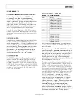
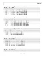
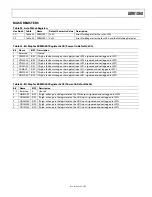
A number of status registers indicate the logic state of all of the
functions controlled by the ADM1060. These logic states
include the output of both the UV and OV comparators of each
of the seven SFDs, the logic output of the SFDs themselves, the
logic state of the GPIs, the error condition on the WDI, and the
logic state of each of the nine PDOs. The content of these
registers, which is read-only, can be read at any time via the
SMBus interface. The register and bit map for each of these
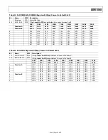
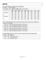
status registers are described in the tables that follow.
FAULT REGISTERS
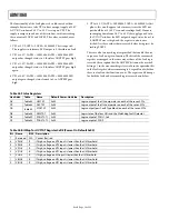
The ADM1060 also provides fault reporting. For example, if a
fault occurs causing a PDO to change its status, the user can
determine what function actually faulted. This is achieved by
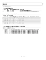
providing a “fault plane” consisting of two registers, LATF1 and
LATF2, that the system controller can read out of the ADM1060
via the SMBus. Each bit in the two registers (with one important
exception, see below) is assigned to one of the inputs of the
devices as shown in Table 41.
Table 41. Fault Plane of ADM1060
Register Bit Assigned
Function
LATF1 7 ANYFLT
6
Logic Output of VP4 SFD
5
Logic Output of VP3 SFD
4
Logic Output of VP2 SFD
3
Logic Output of VP1 SFD
2
Logic Output of VH SFD
1
Logic Output of VB2 SFD
0
Logic Output of VB1 SFD
LATF2 7
6
5
4
Logic Output of WDI
3
Logic Input on GPI4
2
Logic Input on GPI3
1
Logic Input on GPI2
0
Logic Input on GPI1
Each bit represents the logical status of its assigned function,
i.e., the logical output of the SFDs and WDI, and the logic level
on the GPI inputs.
The important exception is the MSB of the LATF1 register. This
is the ANYFLT bit. This bit goes high if one of the other bits in
the two registers faults. A fault is defined as a change in polarity
from the last time the fault registers were read. Once ANYFLT
goes high, the contents of the two registers are latched, thus
preventing more than one of the other bits from changing
polarity before the content of the registers is read. Therefore, the
first faulting input can be determined.
The sequence in which the registers are read is determined by
ANYFLT. As long as ANYFLT remains at 0, only the content of
LATF1 is read. There are two reasons for this. The first is that
ANYFLT = 0 implies that no fault has occurred and, therefore,
there is no need to read the contents of LATF2. The second and
more important reason is that reading register LATF2 actually
resets the ANYFLT bit to 0. Thus, if a fault occurred on an SFD
after LATF1 had been read but before LATF2 had been read,
ANYFLT would change to 1, indicating that a fault had
occurred, but would be reset to 0 once LATF2 was read, thus
erasing the log of the fault. In summary then, LATF2 should
only be read if ANYFLT = 1. Reading the registers in this
sequence ensures that the contents are never reset before a fault
has been logged over the SMBus, thus ensuring that the
supervising processor or CPLD knows what function
supervised by the ADM1060 caused the fault. The faulting
function is determined by comparing the contents of the fault
plane (i.e., the contents of the two registers) with the values read
previously, and determining which bit changed polarity.

