


ADM1060
Rev. B | Page 41 of 52
Table 55. List of Configuration Update Registers
Hex Addr.
Table
Name
Default Power-
On Value
Description
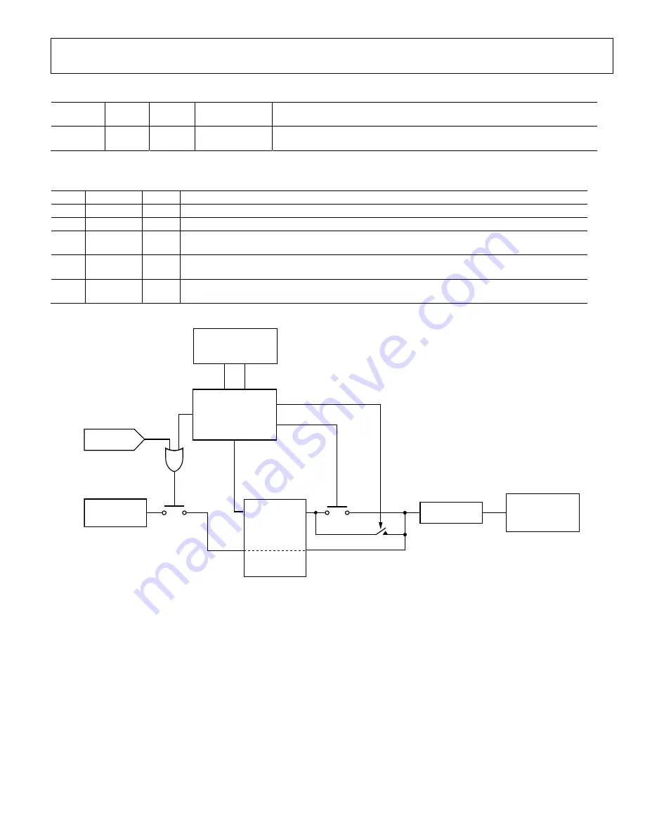
90
Configuration Update Control register for changing configuration of the
ADM1060 after power-up
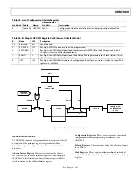
Table 56. Bit Map for UPDCFG Register 0x90 (Power-On Default 0x00)
Bit Name
R/W Description
7–4
Reserved
N/A
Cannot be used
3
EE_ERASE
R/W
If set high, EEPROM page erasure can be programmed.
2 EEPROMLD
W If set high, the ADM1060 will download the contents of its EEPROM to the RAM registers. This bit
self-clears (returns to 0) after the download.
1 RAMLD W If set high, the ADM1060 will download the buffered RAM register data into the local latches. This bit
self-clears (returns to 0) after the download.
0 UPD
R/W
If set high, the ADM1060 will update its configuration in real time as a word is written to a local RAM
register via the SMBus.
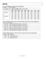
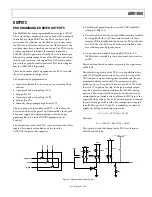
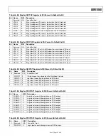
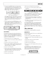
EEPROM
EEPROMLD
POWER-UP
(V
CC
>2.5V)
DEVICE
CONTROLLER
SMBus
LATCH A
DATA
RAMLD
UPD
LATCH B
FUNCTION (E.G.,
OV THRESHOLD
ON VP1)
Figure 24. Configuration Update Flow Diagram
INTERNAL REGISTERS
The ADM1060 contains a large number of data registers. A brief
description of the principal registers is given below. More
detailed descriptions are given in the relevant sections of this
data sheet.
Address Pointer Register.
This register contains the address
that selects one of the other internal registers. When writing to
the ADM1060, the first byte of data is always a register address,
which is written to the Address Pointer register.
Configuration Registers.
These registers provide control and
configuration for various operating parameters of the
ADM1060.
Polarity Registers.
These registers define the polarity of inputs
to the PLBA.
Mask Registers.
These registers allow masking of individual
inputs to the PLBA and masking of faults in the fault reporting
registers.


