ADM1060
Rev. B | Page 11 of 52
INPUTS
POWERING THE ADM1060
The ADM1060 is powered from the highest voltage input on
either the Positive Only supply inputs (VPn) or the High Volt-
age supply input (VH). The same pins are used for supply fault
detection (discussed below). A V
DD
arbitrator on the device
chooses which supply to use. The arbitrator can be considered
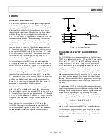
as diode OR’ing the positive supplies together (as shown in
Figure 17).The diodes are supplemented with switches in a syn-
chronous rectifier manner to minimize voltage loss. This loss
can be reduced to ~0.2 V, resulting in the ability to power the
ADM1060 from a supply as low as 3.0 V. Note that the supply on
the VBn pins cannot be used to power the device, even if the
input on these pins is positive. Also, the minimum supply of
3.0 V must appear on one of the VPn pins in order to correctly
power up the ADM1060. A supply of no less than 4.5 V can be
used on VH. This is because there is no synchronous rectifier
circuit on the VH pin, resulting in a voltage drop of ~1.5 V
across the diode of the V
DD
arbitrator.
An external capacitor to GND is required to decouple the
on-chip supply from noise. This capacitor should be connected
to the VDDCAP pin, as shown in Figure 17. The capacitor has
another use during “brown outs” (momentary loss of power).
Under these conditions, where the input supply, VPn, dips
transiently below V
DD
, the synchronous rectifier switch
immediately turns off so that it does not pull V
DD
down. The
V
DD
capacitor can then act as a reservoir to keep the chip active
until the next highest supply takes over the powering of the
device. A 1 µF capacitor is recommended for this function. A
minimum capacitor value of 0.1 µF is required.
Note that in the case where there are two or more supplies
within 100 mV of each other, the supply that takes control of
V
DD
first will keep control. For example, if VP1 is connected to a
3.3 V supply, V
DD
will power up to approximately 3.1 V through
VP1. If VP2 is then connected to another 3.3 V supply, VP1 will
still power the device, unless VP2 goes 100 mV higher than
VP1.
A second capacitor is required on the VCCP pin of the
ADM1060. This capacitor is the reservoir capacitor for the
central charge pump. Again, a 1 µF capacitor is recommended
for this function. A minimum capacitor value of 0.1 µF is
required.
VH
VP1
VP2
VP3
VP4
VDDCAP PIN
OFF-CHIP
DECOUPLING
CAPACITOR
ON-CHIP SUPPLY
Figure 17. V
DD
Arbitrator Operation
PROGRAMMABLE SUPPLY FAULT DETECTORS
(SFDs)
The ADM1060 has seven programmable supply fault detectors
(SFDs): one high voltage detector (+2 V to +14.4 V), two bipolar
detectors (+1 V to +6 V, −2 V to –6 V) and four positive only
voltage detectors (+0.6 V to +6 V). Inputs are applied to these
detectors via the VH (high voltage supply input), VBn (bipolar
supply input), and VPn (positive only input) pins, respectively.
The SFDs detect a fault condition on any of these input supplies.
A fault is defined as undervoltage (where the supply drops
below a preprogrammed level), overvoltage (where the supply
rises above a preprogrammed level), or out-of-window (where
the supply deviates outside either the programmed overvoltage
or undervoltage threshold). Only one fault type can be selected
at a time.
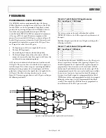
An undervoltage (UV) fault is detected by comparing the input
supply to a programmed reference (the undervoltage threshold).
If the input voltage drops below the undervoltage threshold, the
output of the comparator goes high, asserting a fault. The
undervoltage threshold is programmed using an 8-bit DAC. On
a given range, the UV threshold can be set with a resolution of
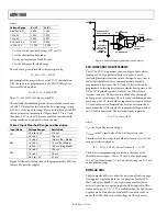
Step Size
=
Threshold Range
/255
An overvoltage (OV) fault is detected in exactly the same way,
using a second comparator and DAC to program the reference.
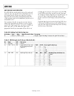
All thresholds are programmed using 8-bit registers, one regis-
ter each for the seven UV thresholds and one each for the seven
OV thresholds. The UV or OV threshold programmed by the
user is given by
B
R
T
V
N
V
V
+
×
=
255


