ADM1060
Rev. B | Page 21 of 52
PROGRAMMING
PROGRAMMABLE LOGIC BLOCK ARRAY
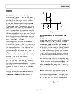
The ADM1060 contains a programmable logic block array
(PLBA). This block is the logical core of the device. The PLBA
(and the PDBs—see the Programmable Delay Block section)
provides the sequencing function of the ADM1060. The asser-
tion of the nine programmable driver outputs (PDO) is
controlled by the PLBA. The PLBA is comprised of nine macro-
cells, one per PDO channel. The main components of the
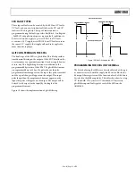
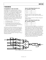
macrocells are two wide AND-OR gates, as shown in Figure 20.
Each AND gate represents a function (A or B) that can be used
independently to control the assertion of the PDO pin. There
are 21 inputs to each of these AND gates:
•
The logic outputs of all seven supply fault detectors
•
The four GPI logic inputs
•
The watchdog fault detector (latched and pulsed)
•
The delayed output of any of the other macrocells (the
output of a macrocell cannot be an input to itself, since this
would result in a nonterminating loop).
All 21 inputs are hardwired to both function A and function B
AND gates. The user can then select which of these inputs con-
trols the output. This is done using two control signals, IMK (a
masking bit, setting it ignores the relevant input) and POL (a
polarity bit, setting it inverts the input before it is applied to the
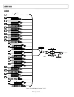
AND gate). The effect of setting these bits can be seen in
Figure 20. The inverting gate shown is an XOR gate, resulting in
the following truth table:
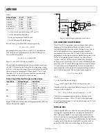
Table 26. Truth Table for PLB Input Inversion
POL Input
Signal XOR
Output
0 0
0
0 1
1
1 0
1
1 1
0
The last two entries in the truth table show that with the
INVERT (POL) bit set, the XOR output is always the inverse of
the input.
Similarly, the ignore gate shown is an OR gate, resulting in the
following truth table:
Table 27. Truth Table for PLB Input Masking
IMK
Input Signal
OR Output
0 0
0
0 1
1
1 0
1
1 1
1
It can be seen here that once the IMK bit is set, the OR output is
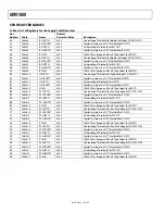
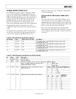
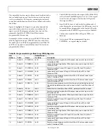
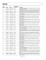
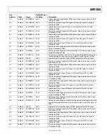
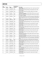
always 1, regardless of the input, thus ignoring it. Figure 21 is a
detailed diagram of the 21 inputs and the registers required to
program them. Those shown are just for function A of PLB1,
but function B and all of the functions in the other eight PLBs
are programmed exactly the same way. An enable register allows
the user to use function A, function B, or both. The output of
functions A and/or B is input to a programmable delay block
(PDB) where a delay can be programmed on both the rising and
falling edges of an input (see the Programmable Delay Block
section). The output of this PDB block can be progammed to
invert before any of the PDO pins is asserted.
INVERT
OUTPUT
PLBOUT
PROGRAMMABLE
DELAY
BLOCK
ENABLE
FUNCTION A
ENABLE
FUNCTION B
2 WIDE AND GATES
(21 INPUTS)
SIGNAL INPUTS
POL (INVERT)
IMK (IGNORE)
Figure 20. Simplified Programmable Logic Block Macrocell Schematic

