ADM1060
Rev. B | Page 3 of 52
GENERAL DESCRIPTION
(continued from Page 1)
All of the inputs and outputs described previously are
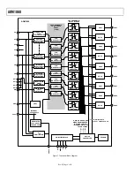
controlled by the programmable logic block array (PLBA). This
is the logic core of the ADM1060. It is comprised of nine
macrocells, one for each PDO. These macrocells are essentially
just wide AND gates. Any/all of the inputs can be used as an
input to these macrocells. The output of a macrocell can also be
used as an input to any macrocell other than itself (an input to
itself would result in a nonterminating loop). The PLBA outputs
control the PDOs of the ADM1060 via delay blocks, where a
delay of 0 ms to 500 ms can be programmed on the rising
and/or the falling edge of the data. This results in a very flexible
sequencing ability. Thus, for instance, PDO1 can be
programmed so that it will not assert until the VP2, VP3, and
VP4 supplies are in tolerance; VB1 and VH have been in
tolerance for 200 ms; and PDO7 has already been asserted. A
simple sequencing operation would be to daisy-chain each PLB
output into the input of the next PLB such that PDO9 does not
assert until PDO8 asserts, which in turn does not assert until
PDO7 asserts, and so on.
All of the functional capability described here is programmable
through the industry-standard 2-wire bus (SMBus) provided.
Device settings can be written to EEPROM memory for auto-
matic programming of the device on power-up. The EEPROM
is organized in 512 bytes, half of which are used to program all
of the functions on the ADM1060. The other 256 bytes of
EEPROM are for general-purpose system use such as date codes
and system ID. Read/write access to this is also via the 2-wire
interface. In addition, each output state can be directly over-
driven from the serial interface, allowing a further level of
control, as in a system controlled soft power-down.


