ADSP-BF59x Blackfin Processor Hardware Reference
6-3
Dynamic Power Management
multiplication range, the processor uses a combination of programmable
dividers in the PLL feedback circuit and output configuration blocks.
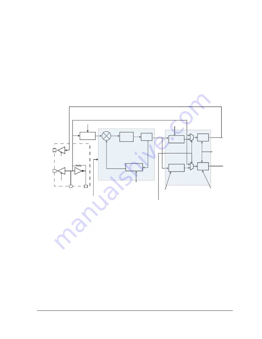
Figure 6-1
illustrates a conceptual model of the PLL circuitry, configura-
tion inputs, and resulting outputs. In the figure, the VCO is an
intermediate clock from which the core clock (
CCLK
) and system clock
(
SCLK
) are derived.
PLL Clock Multiplier Ratios
The PLL control register (
PLL_CTL
) governs the operation of the PLL. For
details about the
PLL_CTL
register, see
“PLL_CTL Register” on page 6-20
.
Figure 6-1. PLL Block Diagram
OUTPUT CLOCK
GENERATOR (CLOCK
DIVIDE AND MUX)
÷1 OR ÷2
LOOP
FILTER
VCO
÷5,..., ÷64
÷1, ÷2, ÷4,
OR ÷8
÷1,..., ÷15
+
-
CLKOUT
CLKBUF
CLKIN
XTAL
SSEL [3:0}
MSEL [5:0]
CSEL [1:0]
EN
EN
DF
SCLK
GATE
GATE
SCLK
CCLK
PDWN
DEEP SLEEP
POWERDOWN
(CCLK AND
SCLK OFF)
STOPCK
(SLEEP MODE)
STOP CLOCK
CCLK OFF
BYPASS
(ACTIVE
MODE)
CCLK = SCLK = CLKIN
PHASE LOCKED LOOP
f
CLKIN
f
CLKIN
f
VCO
PLL_OFF DISABLE
CONTROL INPUT TO PLL.
CAN ADDITIONALLY BE
USED WITH BYPASS
Summary of Contents for ADSP-BF59x Blackfin
Page 64: ...Development Tools 1 22 ADSP BF59x Blackfin Processor Hardware Reference...
Page 74: ...Processor Specific MMRs 2 10 ADSP BF59x Blackfin Processor Hardware Reference...
Page 244: ...Programming Examples 6 40 ADSP BF59x Blackfin Processor Hardware Reference...
Page 700: ...Programming Examples 16 78 ADSP BF59x Blackfin Processor Hardware Reference...
Page 738: ...Boundary Scan Architecture B 8 ADSP BF59x Blackfin Processor Hardware Reference...


