background image

ADSP-BF59x Blackfin Processor Hardware Reference

I-9


Index

dynamic power management, 

1-16

6-1

controller, 

6-2

E

early frame sync, 

14-34

EAV signal, 

15-5

EBIU

and DMA, 

5-4

ECINIT[15:0] field, 

5-86

ECOUNT[15:0] field, 

5-86

edge detection, GPIO, 

7-12

elfloader.exe, 

16-8

ELSI (enable Rx status interrupt) bit, 

11-7

11-27

11-28

EMISO (enable MISO) bit, 

13-35

13-36

emulation, and timer counter, 

8-42

EMU_RUN bit, 

8-41

8-42

8-46

enable Pxn interrupt A bit, 

7-27

enable Pxn interrupt B bit, 

7-27

enabling

interrupts, 

4-5

entire field mode, PPI, 

15-9

EPS (even parity select) bit, 

11-21

ERBFI (enable receive buffer full interrupt) 

bit, 

11-7

11-12

11-26

11-27

ERR_DET (error detected) bit, 

15-29

15-30

ERR_NCOR (error not corrected) bit, 

15-30

errors

DMA, 

5-28

not detected by DMA hardware, 

5-30

startup, and timers, 

8-8

error signals, SPI, 

13-38

 to 

13-41

ERR_TYP[1:0] field, 

8-7

8-40

8-41

8-46

ERR_TYP bits, 

8-28

ETBEI (enable transmit buffer empty 

interrupt) bit, 

11-6

11-11

11-17

11-26

11-27

event controller, 

4-2

event handling, 

4-2

events

definition, 

4-3

types of, 

4-2

event system, 

4-3

event vector table (EVT), 

4-2

EVT1 register, 

16-6

EXT_CLK mode, 

8-32

8-43

control bit and register usage, 

8-45

flow diagram, 

8-33

external

emulator debugger, 

8-42

external crystal, 

1-16

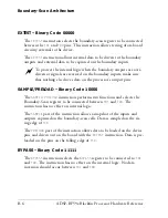
EXTEST instruction, 

B-6

EZ-KIT Lite card, 

1-21

F

FAST (fast mode) bit, 

12-29

12-31

fast mode, TWI, 

12-10

FE (framing error) bit, 

11-24

11-25

FFE (force framing error on transmit) bit, 

11-31

FIFO

asynchronous connection, 

5-38

finish control command, DMA, 

5-33

FLD (field indicator) bit, 

15-30

15-31

FLD_SEL (active field select) bit, 

15-4

15-26

15-29

flex descriptors, 

5-3

FLGx (slave select value) bit, 

13-37

13-38

FLOW[2:0] field, 

5-22

5-23

5-55

5-67

5-68

flow charts

DMA, 

5-18

5-19

general-purpose timers interrupt 

structure, 

8-6

GPIO, 

7-17

GPIO interrupt generation, 

7-14

PPI, 

15-24

SPI core-driven, 

13-29

Summary of Contents for ADSP-BF59x Blackfin

Page 1: ...a ADSP BF59x Blackfin Processor Hardware Reference Revision 1 0 May 2011 Part Number 82 100102 01 Analog Devices Inc One Technology Way Norwood Mass 02062 9106...

Page 2: ...to be accurate and reliable However no responsibility is assumed by Analog Devices for its use nor for any infringement of patents or other rights of third parties which may result from its use No lic...

Page 3: ...l or Customer Support xxxiv Registration for MyAnalog com xxxv EngineerZone xxxv Social Networking Web Sites xxxvi Supported Processors xxxvi Product Information xxxvii Analog Devices Web Site xxxvii...

Page 4: ...Peripheral Interface 1 9 SPORT Controllers 1 11 Serial Peripheral Interface SPI Ports 1 13 Timers 1 13 UART Port 1 14 Watchdog Timer 1 15 Clock Signals 1 16 Dynamic Power Management 1 16 Full On Mode...

Page 5: ...sor Specific MMRs 2 4 DTEST_COMMAND Register 2 5 ITEST_COMMAND Register 2 6 DMEM_CONTROL Register 2 7 IMEM_CONTROL Register 2 7 DCPLB_DATAx Registers 2 8 ICPLB_DATAx Registers 2 9 CHIP BUS HIERARCHY C...

Page 6: ...stem Peripheral Interrupts 4 4 Programming Model 4 7 System Interrupt Initialization 4 7 System Interrupt Processing Summary 4 8 System Interrupt Controller Registers 4 10 System Interrupt Assignment...

Page 7: ...Memory DMA 5 6 Handshaked Memory DMA HMDMA Mode 5 8 Modes of Operation 5 9 Register Based DMA Operation 5 9 Stop Mode 5 11 Autobuffer Mode 5 11 Two Dimensional DMA Operation 5 11 Examples of Two Dime...

Page 8: ...estart or Finish 5 35 Handshaked Memory DMA Operation 5 36 Pipelining DMA Requests 5 37 HMDMA Interrupts 5 39 DMA Performance 5 40 DMA Throughput 5 41 Memory DMA Timing Details 5 44 Static Channel Pri...

Page 9: ...IG MDMA_yy_CONFIG 5 67 DMA Interrupt Status Registers DMAx_IRQ_STATUS MDMA_yy_IRQ_STATUS 5 71 DMA Start Address Registers DMAx_START_ADDR MDMA_yy_START_ADDR 5 74 DMA Current Address Registers DMAx_CUR...

Page 10: ...isters HMDMAx_CONTROL 5 82 Handshake MDMA Initial Block Count Registers HMDMAx_BCINIT 5 84 Handshake MDMA Current Block Count Registers HMDMAx_BCOUNT 5 84 Handshake MDMA Current Edge Count Registers H...

Page 11: ...NAMIC POWER MANAGEMENT Phase Locked Loop and Clock Control 6 1 PLL Overview 6 2 PLL Clock Multiplier Ratios 6 3 Core Clock System Clock Ratio Control 6 5 Dynamic Power Management Controller 6 7 Operat...

Page 12: ...tem Control ROM Function in C C 6 24 Accessing the System Control ROM Function in Assembly 6 25 Programming Examples 6 28 Full on Mode to Active Mode and Back 6 30 Transition to Sleep Mode or Deep Sle...

Page 13: ...19 PORTx Pad Control Registers 7 19 Memory Mapped GPIO Registers 7 20 Port Multiplexer Control Register PORTx_MUX 7 21 Function Enable Registers PORTx_FER 7 22 GPIO Direction Registers PORTxIO_DIR 7...

Page 14: ...xamples 7 33 GENERAL PURPOSE TIMERS Specific Information for the ADSP BF59x 8 1 Overview 8 2 External Interface 8 3 Internal Interface 8 4 Description of Operation 8 4 Interrupt Processing 8 5 Illegal...

Page 15: ...Register TIMER_STATUS 8 38 Timer Configuration Register TIMER_CONFIG 8 40 Timer Counter Register TIMER_COUNTER 8 41 Timer Period TIMER_PERIOD and Timer Width TIMER_WIDTH Registers 8 42 Summary 8 45 P...

Page 16: ...the ADSP BF59x Processor 9 9 WATCHDOG TIMER Specific Information for the ADSP BF59x 10 1 Overview and Features 10 1 Interface Overview 10 3 External Interface 10 3 Internal Interface 10 3 Description...

Page 17: ...peration 11 7 IrDA Transmit Operation 11 8 IrDA Receive Operation 11 9 Interrupt Processing 11 11 Bit Rate Generation 11 12 Autobaud Detection 11 13 Programming Model 11 15 Non DMA Mode 11 15 DMA Mode...

Page 18: ...gramming Examples 11 32 Unique Information for the ADSP BF59x Processor 11 41 TWO WIRE INTERFACE CONTROLLER Specific Information for the ADSP BF59x 12 1 Overview 12 2 Interface Overview 12 3 External...

Page 19: ...g 12 17 Clock Stretching During FIFO Underflow 12 17 Clock Stretching During FIFO Overflow 12 19 Clock Stretching During Repeated Start Condition 12 20 Programming Model 12 22 Register Descriptions 12...

Page 20: ...Transmit Data Single Byte Register TWI_XMT_DATA8 12 43 TWI FIFO Transmit Data Double Byte Register TWI_XMT_DATA16 12 43 TWI FIFO Receive Data Single Byte Register TWI_RCV_DATA8 12 44 TWI FIFO Receive...

Page 21: ...ultiple Slave SPI Systems 13 8 Internal Interfaces 13 10 DMA Functionality 13 10 Description of Operation 13 11 SPI Transfer Protocols 13 11 SPI General Operation 13 14 Clock Signals 13 15 Interrupt O...

Page 22: ...Error TXCOL 13 41 SPI Transmit Data Buffer SPI_TDBR Register 13 41 SPI Receive Data Buffer SPI_RDBR Register 13 42 SPI RDBR Shadow SPI_SHADOW Register 13 43 Programming Examples 13 43 Core Generated...

Page 23: ...10 Stereo Serial Operation 14 10 Multichannel Operation 14 14 Multichannel Enable 14 17 Frame Syncs in Multichannel Mode 14 18 The Multichannel Frame 14 19 Multichannel Frame Delay 14 20 Window Size 1...

Page 24: ...yncs 14 32 Sampling Edge for Data and Frame Syncs 14 32 Early Versus Late Frame Syncs Normal Versus Alternate Timing 14 34 Data Independent Transmit Frame Sync 14 36 Moving Data Between SPORTs and Mem...

Page 25: ...on SPORT_MCMC1 and SPORT_MCMC2 Registers 14 63 SPORT Current Channel SPORT_CHNL Register 14 64 SPORT Multichannel Receive Selection SPORT_MRCSn Registers 14 65 SPORT Multichannel Transmit Selection SP...

Page 26: ...5 5 ITU R 656 Modes 15 5 ITU R 656 Background 15 5 ITU R 656 Input Modes 15 9 Entire Field 15 9 Active Video Only 15 10 Vertical Blanking Interval VBI only 15 10 ITU R 656 Output Mode 15 11 Frame Sync...

Page 27: ...egister PPI_CONTROL 15 25 PPI Status Register PPI_STATUS 15 29 PPI Delay Count Register PPI_DELAY 15 32 PPI Transfer Count Register PPI_COUNT 15 32 PPI Lines Per Frame Register PPI_FRAME 15 33 Program...

Page 28: ...18 Using HWAIT as Reset Indicator 16 19 Boot Termination 16 19 Single Block Boot Streams 16 20 Advanced Boot Techniques 16 21 Initialization Code 16 21 Quick Boot 16 25 Indirect Booting 16 26 Callbac...

Page 29: ...Boot Mode 16 47 UART Slave Mode Boot 16 49 L1 ROM Boot Mode 16 51 Reset and Booting Registers 16 51 Software Reset SWRST Register 16 52 System Reset Configuration SYSCR Register 16 54 Boot Code Revisi...

Page 30: ...1 System Reset 16 71 Exiting Reset to User Mode 16 72 Exiting Reset to Supervisor Mode 16 72 Initcode Power Management Control 16 73 XOR Checksum 16 75 SYSTEM DESIGN Pin Descriptions 17 1 Managing Clo...

Page 31: ...e 17 9 SYSTEM MMR ASSIGNMENTS Processor Specific Memory Registers A 2 Core Timer Registers A 3 System Reset and Interrupt Control Registers A 3 DMA Memory DMA Control Registers A 4 Ports Registers A 7...

Page 32: ...Reference TEST FEATURES JTAG Standard B 1 Boundary Scan Architecture B 2 Instruction Register B 4 Public Instructions B 5 EXTEST Binary Code 00000 B 6 SAMPLE PRELOAD Binary Code 10000 B 6 BYPASS Bina...

Page 33: ...all features and processes that they support For program ming information see the Blackfin Processor Programming Reference For timing electrical and package specifications see the ADSP BF592 Black fin...

Page 34: ...ough the system Chapter 4 System Interrupts Describes the system peripheral interrupts including setup and clearing of interrupt requests Chapter 5 Direct Memory Access Describes the peripheral DMA an...

Page 35: ...s I2C Bus Specification version 2 1 dated January 2000 Chapter 13 SPI Compatible Port Controller Describes the Serial Peripheral Interface SPI port that provides an I O interface to a variety of SPI c...

Page 36: ...the processor discusses the JTAG stan dard boundary scan architecture instruction and boundary registers and public instructions This hardware reference is a companion document to the Blackfin Process...

Page 37: ...free feature of the Analog Devices Web site that allows customization of a Web page to display only the latest information about products you are interested in Click Register to use this site Registra...

Page 38: ...LinkedIn Network with the LinkedIn group Analog Devices SHARC http www linkedin com Supported Processors The following is the list of Analog Devices Inc processors supported in VisualDSP Blackfin ADS...

Page 39: ...d digital signal processors To access a complete technical library for each processor family go to http www analog com processors technical_library The manuals selection opens a list of current manual...

Page 40: ...ollows Technical Library CD The technical library CD contains seminar materials product highlights a selection guide and documentation files of processor manuals VisualDSP software manuals and hardwar...

Page 41: ...the Close com mand appears on the File menu this that Alternative required items in syntax descriptions appear within curly brackets and separated by vertical bars read the example as this or that One...

Page 42: ...ould lead to undesirable results or product damage In the online version of this book the word Caution appears instead of this symbol Warning Injury to device users may result if A Warning identifies...

Page 43: ...ne a dual MAC state of the art signal processing engine the advantages of a clean orthogonal RISC like micro processor instruction set and single instruction multiple data SIMD multimedia capabilities...

Page 44: ...ation to significantly lower overall power consumption This capability can result in a substantial reduction in power consumption compared with just Table 1 1 Processor Features Feature ADSP BF592 Tim...

Page 45: ...hree 32 bit timer counters with PWM support 32 bit core timer On chip PLL capable of 5 to 64 frequency multiplication Debug JTAG interface Parallel Peripheral Interface PPI supporting ITU R 656 video...

Page 46: ...a single unified 4G byte address space using 32 bit addresses All resources including internal memory external memory and I O control registers occupy sep arate sections of this common address space...

Page 47: ...L1 scratchpad RAM which runs at the same speed as the L1 mem ories but is only accessible as data SRAM L1 instruction ROM memory accessed at full processor speed I O Memory Space Blackfin processors...

Page 48: ...ach individual DMA capable peripheral has at least one dedicated DMA channel The DMA controller supports both one dimensional 1D and two dimensional 2 D DMA transfers DMA transfer initialization can b...

Page 49: ...with other ADSP BF59x processor peripherals via a multi plexing scheme however the GPIO functionality is the default state of the device upon powerup Neither GPIO output or input drivers are active b...

Page 50: ...edge sensitive whether just the ris ing edge or both the rising and falling edges of the signal are significant One register selects the type of sensitivity and one reg ister selects which edges are s...

Page 51: ...he OmniVision Serial Camera Control Bus SCCB Functional Specification version 2 1 Parallel Peripheral Interface The processor provides a Parallel Peripheral Interface PPI that can con nect directly to...

Page 52: ...in horizontal and vertical blanking intervals Though not explicitly supported ITU R 656 output functionality can be achieved by setting up the entire frame structure including active video blanking an...

Page 53: ...ions The SPORTs support these features Bidirectional I2S capable operation Each SPORT has two sets of independent transmit and receive pins which enable eight channels of I2 S stereo audio Buffered ei...

Page 54: ...an be selected on the transmit and or receive channel of the SPORT without addi tional latencies DMA operations with single cycle overhead Each SPORT can automatically receive and transmit multiple bu...

Page 55: ...DMA controller configurable to support either transmit or receive datastreams The SPI s DMA controller can only ser vice unidirectional accesses at any given time During transfers the SPI port simult...

Page 56: ...The UART port provides a simplified UART interface to other peripherals or hosts providing half duplex DMA supported asynchronous transfers of serial data The UART port includes support for 5 to 8 dat...

Page 57: ...function A software watchdog can improve system availability by forcing the processor to a known state through generation of a hardware reset nonmaskable interrupt NMI or general purpose interrupt if...

Page 58: ...p PLL is capable of multiplying the CLKIN signal by a user programmable 5 to 64 multiplication factor bounded by specified minimum and maxi mum VCO frequencies The default multiplier is 6 but it can b...

Page 59: ...ode is entered DMA access is available to appropriately config ured L1 memories In the active mode it is possible to disable the PLL through the PLL con trol register PLL_CTL If disabled the PLL must...

Page 60: ...Although not strictly an operating mode like the four modes detailed above it is illustrative to view it as such Instruction Set Description The Blackfin processor family assembly language instruction...

Page 61: ...byte memory space providing a simplified programming model Code density enhancements include intermixing of 16 and 32 bit instructions with no mode switching or code segregation Frequently used instr...

Page 62: ...oints Set conditional breakpoints on registers memory and stacks Trace instruction execution Perform linear or statistical profiling of program execution Fill dump and graphically plot the contents of...

Page 63: ...ualDSP development environ ment but can also be used with standard command line tools The VDK development environment assists in managing system resources automat ing the generation of various VDK bas...

Page 64: ...Development Tools 1 22 ADSP BF59x Blackfin Processor Hardware Reference...

Page 65: ...cache Memory Architecture Figure 2 1 on page 2 2 provides an overview of the ADSP BF59x proces sor system memory map For a detailed discussion of how to use them see the Blackfin Processor Programming...

Page 66: ...subbanks Figure 2 1 ADSP BF59x Memory Map Table 2 1 L1 Instruction Memory Subbanks Memory Bbank Memory Subbank Memory Start Location for ADSP BF59x Processors Instruction Bank A 0 0xFFA0 0000 Instruc...

Page 67: ...naled by hardware DMA access of instruction ROM is not possible L1 Data SRAM Table 2 2 shows how the subbank organization is mapped into memory Instruction Bank A 2 0xFFA0 2000 Instruction Bank A 3 0x...

Page 68: ...in Chapter 16 System Reset and Booting External Memory Aside from the Boot ROM which sits in External Memory space there is no additional external memory address space on the processor Processor Speci...

Page 69: ...27 26 25 24 23 22 21 20 19 18 17 16 X X X X X X X X X X X X X X X Data Test Command Register DTEST_COMMAND Address bits 13 12 ADR 13 12 Reset Undefined Read Write Access ADR 11 Address bit 11 REGION 2...

Page 70: ...s 0xFFA07FFF All other regions of L1 memory both data and instruction are accessed using the DTEST_COMMAND register Figure 2 3 Instruction Test Command Register X 31 30 29 28 27 26 25 24 23 22 21 20 1...

Page 71: ...9 18 17 16 0 0 0 0 0 0 0 0 0 0 0 0 0 0 0 Data Memory Control Register DMEM_CONTROL Reset 0x00000001 ENDCPLB Data Cacheability Protection Lookaside Buffer Enable 0 CPLBs disabled Minimal address checki...

Page 72: ...lid disabled CPLB entry 1 Valid enabled CPLB entry CPLB_USER_WR 0 Write access prohibited in User Mode writes generate protection violation exceptions 1 Write access permitted in User Mode CPLB_SUPV_W...

Page 73: ...ction CPLB Data Registers ICPLB_DATAx 00 1K byte page 01 4K byte page 10 1M byte page 11 4M byte page PAGE_SIZE1 0 Reset 0x00000000 CPLB_VALID 0 Invalid disabled CPLB entry 1 Valid enabled CPLB entry...

Page 74: ...Processor Specific MMRs 2 10 ADSP BF59x Blackfin Processor Hardware Reference...

Page 75: ...on page 3 1 Interface Overview on page 3 2 Chip Bus Hierarchy Overview ADSP BF59x Blackfin processors feature a powerful chip bus hierarchy on which all data movement between the processor core intern...

Page 76: ...igure 3 1 shows the core processor and system boundaries as well as the interfaces between them Figure 3 1 Processor Bus Hierarchy GPIOS SPORTs SPIs BOOT ROM PPI UART TIMERS DMA CONTROLLER L1 SRAM L1...

Page 77: ...o allow the core processor to run at an optimal frequency Note all synchronous peripherals derive their timing from the SCLK For example the UART clock rate is determined by further divid ing this clo...

Page 78: ...s accessed through the PAB are mapped into the system MMR space of the processor memory map The core accesses system MMR space through the PAB bus Figure 3 2 Core Block Diagram INT RESET VECTOR ACK CO...

Page 79: ...arbitration is necessary PAB Agents Masters Slaves The processor core can master bus operations on the PAB All peripherals have a peripheral bus slave interface which allows the core to access con tro...

Page 80: ...s for DMA capable peripherals to gain access to on chip memory with little or no degradation in core bandwidth to memory DAB and DCB Arbitration Thirteen DMA channels and bus masters support the DMA c...

Page 81: ...o the DAB s pipelined design Bus arbitration cycles are concurrent with the previous DMA access s data cycles SPORT0 transmit 2 SPORT1 receive 3 SPORT1 transmit 4 SPI0 transmit receive 5 SPI1 transmit...

Page 82: ...s and the DMA access are not to the same memory bank 4K byte size for L1 If there is a conflict DMA is the highest priority requester followed by the core Note that a locked transfer by the core proce...

Page 83: ...t please refer to the ADSP BF592 Blackfin Processor Data Sheet To determine how each of the system interrupts is multiplexed with other functional pins refer to Table 7 1 on page 7 3 through Table 7 2...

Page 84: ...masks groups and prioritizes interrupt requests sig nalled by on chip or off chip peripherals and forwards them to the CEC Description of Operation The following sections describe the operation of the...

Page 85: ...onsequently several service routines may be active at any time and a low priority event may be pre empted by one of higher priority The CEC supports nine general purpose interrupts IVG7 IVG15 in addit...

Page 86: ...grams their priority by assigning them to individual IVG chan nels However the relative priority of peripheral interrupts can be set by mapping the peripheral interrupt to the appropriate general purp...

Page 87: ...ects the interrupt the bit is asserted When the SIC detects that the peripheral interrupt input has been deas serted the respective bit in the system interrupt status register is cleared Note for some...

Page 88: ...age 4 11 show the default DMA assignment Once a peripheral has been assigned to any other DMA chan nel it uses the new DMA channel s interrupt ID regardless of whether DMA is enabled or not Therefore...

Page 89: ...enerate an interrupt The peripheral interrupt structure of the processor is flexible Upon reset multiple peripheral interrupts share a single general purpose interrupt in the core by default as shown...

Page 90: ...ould wake up the core from an idled state based on this interrupt request 3 SIC_IMASK masks off or enables interrupts from peripherals at the system level If interrupt A is not masked the request proc...

Page 91: ...nterrupt A or if the process of servicing the interrupt clears this bit It should be noted that emulation reset NMI and exception events as well as hardware error IVHW and core timer IVTMR interrupt r...

Page 92: ...in supervisor mode It is advisable however to configure them in the reset interrupt service routine before enabling interrupts To prevent spurious or lost interrupt activity these registers should be...

Page 93: ...n SIC_IAR IVG7 0 IVG8 1 IVG9 2 IVG10 3 IVG11 4 IVG12 5 IVG13 6 IVG14 7 IVG15 8 15 14 13 12 11 10 9 8 7 6 5 4 3 2 1 0 0 0 0 0 0 0 0 0 0 0 0 0 0 0 0 0 System Interrupt Assignment Register SIC_IAR ID Gro...

Page 94: ...are asserted but not yet serviced A 0 in a bit position indicates that a particular inter rupt is deasserted A 1 indicates that it is asserted Refer to Table 4 1 on page 4 3 and Table 4 2 on page 4 1...

Page 95: ...ps requesting the respective ILAT bit is set again immediately and the service routine is invoked again as soon as its first run terminates by an RTI instruction Every software routine that services p...

Page 96: ...epending on system load and instruction history The program sequencer does not wait until the instruction completes and con tinues program execution immediately The SSYNC instruction ensures that the...

Page 97: ...n a single pass or to service them one by one If only one request is serviced and the respective request is cleared by soft ware before the RTI instruction executes the same service routine is invoked...

Page 98: ...TIMER HARDWARE ERROR EXCEPTIONS NMI SIC_IAR3 SIC_IAR2 SIC_IAR1 SIC_IAR0 8 9 10 11 12 13 14 15 16 17 18 19 20 21 22 23 24 25 26 27 28 29 30 31 SIC_ISR0 SIC_IWR0 SIC_IMASK0 RESET EMULATION IMASK IPEND I...

Page 99: ...pt service routine that supports multiple interrupt sources must interrogate the appropriate system memory mapped registers MMRs to determine which peripheral generated the interrupt Table 4 3 Periphe...

Page 100: ...IAR1 19 16 DMA4 SPORT1 TX IVG9 11 Bit 11 SIC_IAR1 15 12 DMA3 SPORT1 RX IVG9 10 Bit 10 SIC_IAR1 11 8 DMA2 SPORT0 TX IVG9 9 Bit 9 SIC_IAR1 7 4 DMA1 SPORT0 RX IVG9 8 Bit 8 SIC_IAR1 3 0 DMA0 PPI IVG8 7 Bi...

Page 101: ...see the appropriate peripheral chapter for additional information Perfor mance and bus arbitration for DMA operations can be found in Chapter 3 Chip Bus Hierarchy Specific Information for the ADSP BF...

Page 102: ...an perform several types of data transfers Peripheral DMA transfers data between memory and on chip peripherals Memory DMA MDMA transfers data between memory and memory The processor has two MDMA modu...

Page 103: ...transfer allows the chaining together of multiple DMA sequences In descriptor based DMA operations a DMA channel can be programmed to automatically set up and start another DMA transfer after the curr...

Page 104: ...EBIU can also be accessed by peripheral DMA or mem ory DMA operation This is typically flash memory SRAM SDRAM FIFOs or memory mapped peripheral devices For products with handshaking MDMA HMDMA the op...

Page 105: ...ternal memories and devices It operates at SCLK frequency Transferred data can be 8 16 or 32 bits wide The DMA controller however connects only to 16 bit buses Memory DMA can pass data every SCLK cycl...

Page 106: ...nnel is disabled DMA requests are ignored and no DMA grants are issued The DMA requests are also not forwarded from the peripheral to the interrupt controller All peripheral DMA channels work complete...

Page 107: ...orities 12 through 15 Priority 12 MDMA0 destination Priority 13 MDMA0 source Priority 14 MDMA1 destination Priority 15 MDMA1 source MDMA0 takes precedence over MDMA1 unless round robin scheduling is u...

Page 108: ...l DMA The DMAx_CONFIG register for the source channel must be written before the DMAx_CONFIG register for the destination channel Handshaked Memory DMA HMDMA Mode This feature is not available for all...

Page 109: ...For best throughput DMA requests can be pipelined The HMDMA controllers feature a request counter to decouple request timing from the data transfers See Handshaked Memory DMA Operation on page 5 36 fo...

Page 110: ...DMAs and destination channel MDMAs set this bit because they write to memory The WDSIZE bit controls the data word width for the trans fer It can be 8 16 or 32 bits wide The DI_EN bit enables an inter...

Page 111: ...ter for details Autobuffer Mode In autobuffer mode the DMA operates repeatedly in a circular manner If all data words have been transferred the address pointer DMAx_CURR_ADDR is reloaded automatically...

Page 112: ...ch decrement of the DMAx_CURR_Y_COUNT register However the DMAx_Y_MODIFY value is not applied to the last item in the array on which the outer loop count DMAx_CURR_Y_COUNT also expires by decrementing...

Page 113: ...egative DMAx_Y_COUNT N M This produces the following address offsets from the start address 0 N M 2 N M 1 N M 1 2 N M 1 2 N M 2 2 N M 2 N M 1 2 N M 1 3 N M 1 Descriptor based DMA Operation In descript...

Page 114: ...om the address pointed to by the DMAx_NEXT_DESC_PTR register The fetch overwrites the DMAx_CONFIG register again If the DMAEN bit is still set the channel starts DMA processing The DFETCH bit in the D...

Page 115: ...e NDSIZE field in the configuration word specifies how many 16 bit words of the next descriptor need to be loaded on the next fetch In descriptor based operation NDSIZE must be non zero The descriptor...

Page 116: ...he DCB bus or the DEB bus and the external memory interface so it is best to keep the size of descriptors as small as possible Mixing Flow Modes The FLOW mode of a DMA is not a global setting If the D...

Page 117: ...mode Before initiating DMA for the first time on a given channel all parameter registers must be initialized Be sure to initialize the upper 16 bits of the DMAx_NEXT_DESC_PTR or DMAx_CURR_DESC_PTR reg...

Page 118: ...H COUNTERS B COPY NEXT DESCRIPTOR POINTER TO CURRENT DESCRIPTOR POINTER USER WRITES SOME OR ALL DMA PARAMETER REGISTERS AND THEN WRITES DMA_CONFIG SET DFETCH IN IRQ_STATUS SET DMA_RUN IN IRQ_STATUS BA...

Page 119: ...OUNTS EXPIRE TEST DI_EN TEST FLOW TEST SYNC WNR DMA STOPPED CLEAR DMA_RUN IN IRQ_STATUS MEMORY WRITE DESTINATION SYNC 0 MEMORY READ FLOW 0 DI_EN 0 DI_EN 1 SIGNAL AN INTERRUPT TO THE CORE SET DMA_DONE...

Page 120: ...OW value determines whether to load more cur rent registers from descriptor elements in memory while the NDSIZE bits detail how many descriptor elements to fetch before starting DMA DMA registers not...

Page 121: ...descriptor from memory After the above steps DMA data transfer operation begins The DMA channel immediately attempts to fill its FIFO subject to channel prior ity a memory write RX DMA channel begins...

Page 122: ...ion by clearing the DMA_RUN bit in DMAx_IRQ_STATUS register after all data in the chan nel s DMA FIFO has been transferred to the peripheral During the fetch in FLOW modes 4 6 and 7 the DMA controller...

Page 123: ...ESC_PTR The first descriptor element that is loaded is a new 32 bit value for the full DMAx_NEXT_DESC_PTR fol lowed by the rest of the descriptor elements The high 16 bits of DMAx_NEXT_DESC_PTR may di...

Page 124: ...ransitions SYNC 0 the DMA FIFO pipeline continues to transfer data to and from the peripheral or destination memory during the descriptor fetch and or when the DMA channel is paused between descriptor...

Page 125: ...eral continuously during the descriptor fetch latency period When SYNC 0 the final interrupt if enabled occurs when the last data is read from memory This interrupt is at the earliest time that the ou...

Page 126: ...MA transmit operation When the interrupt service routine is invoked the DMA_DONE bit is set and the DMA_RUN bit is cleared A synchronized transition also allows greater flexibility in the format of th...

Page 127: ...memory Any prior data items transferred from the peripheral to the DMA FIFO before this register write are discarded This provides direct synchronization between the data stream received from the peri...

Page 128: ...erminate DMA gracefully without DMA abort If a channel has been stopped abruptly by writing DMAx_CONFIG to 0 or any value with DMAEN 0 the user must ensure that any mem ory read or write accesses in t...

Page 129: ...MAx_IRQ_STATUS register to look for a channel with the DMA_ERR bit set bit 1 Clear the problem with that channel for example fix register values Clear the DMA_ERR bit write DMAx_IRQ_STATUS with bit 1...

Page 130: ...rred Either an access attempt was made to an internal address not populated or defined as cache or an external access caused an error signaled by the external memory interface Some prohibited situatio...

Page 131: ...st of three wires per DMA management capable peripheral The DMA control commands extend the set of operations available to the peripheral beyond the simple request data command used by peripherals in...

Page 132: ...emory read receives a Restart command the channel momentarily pauses while any pending memory reads initiated prior to the Restart command are completed During this period of time the channel does not...

Page 133: ...lected by the DI_EN bit The peripheral can thus use the Finish command to partition the DMA stream into work units on its own perhaps as a result of parsing the data currently passing though its suppo...

Page 134: ...fetch memory accesses A DMA management capable peripheral might use this command if an internal FIFO is approaching a critical condition Restrictions The proper operation of the 4 location DMA channe...

Page 135: ...r in the current work unit If five data transfers have been performed then at least one data item has been written to memory in the current work unit which implies that the cur rent work unit s descri...

Page 136: ...ables handshake mode for MDMA1 It is important to understand that the handshake hardware works com pletely independently from the descriptor and autobuffer capabilities of the MDMA allowing most flexi...

Page 137: ...egister returns zero Software can force a reload of the HMDMAx_BCOUNT from the HMDMAx_BCINIT register even during normal operation by setting the RBC bit in the HMDMAx_CONTROL register Set RBC when th...

Page 138: ...ous FIFO could be connected In such a scenario the REP bit should be cleared to let the DMARx request pin listen to falling edges The Blackfin processor does not evaluate the full flag such FIFOs usua...

Page 139: ...which corre sponds to half the FIFO depth Then the MDMA does not start consuming data as long as the FIFO is not half filled On internal system buses memory DMA channels have lower priority than other...

Page 140: ...sh old register called HMDMA_ECOVERFLOW It resets to 0xFFFF and should be written with any positive value by the user before enabling the function by the OIE bit Then the overflow interrupt is issued...

Page 141: ...emory The Chip Bus Hierarchy chapter explains the bus architecture Each peripheral DMA channel has its own data FIFO which lies between the DAB bus and the memory buses These FIFOs automatically prefe...

Page 142: ...elays for example when both the core and the DMA access the same L1 bank when SDRAM pages need to be opened closed or when cache lines are filled Direction changes from RX to TX on the DAB bus impose...

Page 143: ...or s traffic control features described in the next section The MDMA channels are clocked by SCLK If the source and destination are in different memory spaces one internal and one external the inter n...

Page 144: ...s 8 location FIFO After a latency of two SCLK cycles the destination MDMA channel begins writing data to the destination memory buffer Static Channel Prioritization DMA channels are ordinarily granted...

Page 145: ...place before the end of the peripheral s regular interval system failure may result To minimize this possibility the DMA unit detects peripherals whose need for data has become urgent and preferential...

Page 146: ...rgent request may be accommodated The preferential handling of urgent DMA transfers is completely auto matic No user controls are required for this function to operate Memory DMA Priority and Scheduli...

Page 147: ...h For example one stream might be programmed for internal to external moves while the other is programmed for exter nal to internal moves and each would be allocated approximately equal data bandwidth...

Page 148: ...pherals that are request ing DMA via the DAB bus and whose data FIFOs are ready to handle the transfer compete with each other for DAB bus cycles Similarly but sepa rately channels whose FIFOs need me...

Page 149: ...the opposite flow direction These directional preferences work as if the priority of the opposite direction channels were decreased by 16 For example if channels 3 and 5 were requesting DAB access but...

Page 150: ...ral can use a linked descriptor list interrupt driven scheme while another peripheral can simultaneously use a demand driven buffer at a time scheme syn chronized by polling of the DMAx_IRQ_STATUS reg...

Page 151: ...slow operation of channel A Software monitoring of channel B based on examination of the DMAx_CURR_ADDR register contents would not safely conclude whether the memory location pointed to by channel B...

Page 152: ...wait for an interrupt or consult the channel s DMAx_IRQ_STATUS register to confirm completion of DMA rather than polling current address pointer count registers When the DMA system issues an interrup...

Page 153: ...ing scheme using either one or two dimensional indexing with zero proces sor and DMA overhead for looping Synchronization options include 1 D interrupt driven software is interrupted at the conclusion...

Page 154: ...uffer is currently being transferred and then allow one full sub buffer to account for pipelining For example if a read of Table 5 4 2 D Interrupt Driven Double Buffered DMA Register Setting DMAx_STAR...

Page 155: ...ample if a packet of data is to be transmitted from several different locations in memory a header from one location a payload from a list of several blocks of mem ory managed by a memory pool allocat...

Page 156: ...an be set up Descriptor Queue Management A system designer might want to write a DMA manager facility which accepts DMA requests from other software The DMA manager software does not know in advance w...

Page 157: ...he DMA channel is paused after having processed all the descriptors When each new work request is received the DMA manager software ini tializes a new descriptor taking care to write a DMAx_CONFIG val...

Page 158: ...s DMA interrupts to be dropped An interrupt handler capable of safely synchronizing multiple descriptors interrupts would need to be complex performing several MMR accesses to ensure robust operation...

Page 159: ...tly modify the contents of the active descriptor queue unless careful synchronization measures are taken In the most straightforward implementation of a descriptor queue the DMA manager software would...

Page 160: ...MA_RUN bit clears it is safe to restart the DMA by simply writing again to the DMAx_CONFIG register The DMA sequence is repeated with the previous settings Similarly a descriptor based DMA sequence th...

Page 161: ...oid polling of the DMA_RUN bit set the SYNC bit in case of memory read DMAs DMA transmit or MDMA source If all DMACFG fields in a descriptor chain have the FLOW and NDSIZE fields set to zero the indiv...

Page 162: ...afterward Software triggered descriptor fetches are illustrated in Listing 5 7 on page 5 96 MDMA channels can be paused by software at any time by writing a 0 to the DRQ bit field in the HMDMAx_CONTRO...

Page 163: ...Start address of current buffer Parame ter SAH upper 16 bits SAL lower 16 bits 0x08 CONFIG DMA Configuration register including enable bit Parame ter DMACFG 0x0C Reserved Reserved 0x10 X_COUNT Inner l...

Page 164: ...neric MMR names shown in Table 5 6 are not actually mapped to resources in the processor For convenience discussions in this chapter use generic non peripheral specific DMA and memory DMA register nam...

Page 165: ...Ax_PERIPHERAL_MAP All DMA registers can be accessed as 16 bit entities However the follow ing registers may also be accessed as 32 bit registers DMAx_NEXT_DESC_PTR DMAx_START_ADDR DMAx_CURR_DESC_PTR D...

Page 166: ...e that channels 6 and 7 are involved 1 Make sure DMA is disabled on channels 6 and 7 2 Write DMA6_PERIPHERAL_MAP with 0x7000 and DMA7_PERIPHERAL_MAP with 0x6000 3 Enable DMA on channels 6 and or 7 Fig...

Page 167: ...riptor list small model 0x7 Descriptor list large model DMA Configuration Registers DMAx_CONFIG MDMA_yy_CONFIG NDSIZE 3 0 Flex Descriptor Size Size of next descriptor 0000 Required if in Stop or Autob...

Page 168: ...emory are used Instead DMA is performed in a continuous circular buffer fashion based on user programmed DMA MMR settings Upon completion of the work unit the parameter registers are reloaded into the...

Page 169: ...ta interrupt timing select This bit specifies the timing of a data interrupt after completing the whole buffer or after completing each row of the inner loop This bit is used only in 2 D DMA operation...

Page 170: ...sters must be a multiple of the transfer unit size one for 8 bit two for 16 bit four for 32 bit Only SPORT DMA and Memory DMA can operate with a transfer size of 32 bits All other peripherals have a m...

Page 171: ...ipheral there may be up to four data words in the channel s DMA FIFO when the interrupt occurs At this point it is normal to immediately start the next work unit If however the application needs to kn...

Page 172: ...his DMA channel is disabled or it is enabled but paused FLOW mode 0 1 This DMA channel is enabled and operating either transferring data or fetching a DMA descriptor DMA Interrupt Status Registers DMA...

Page 173: ...ster or SIC_IMASK register so that no unintended interrupt is generated on the shared DMA interrupt request line Table 5 7 Data Driven Interrupts Interrupt Name Description No Interrupt Interrupts can...

Page 174: ...sent DMA transfer address for a given DMA session On the first mem ory transfer of a DMA work unit the DMAx_CURR_ADDR register is loaded from the DMAx_START_ADDR register and it is incremented as each...

Page 175: ...6 X Current Address 31 16 X X X X X X X X X X X X X X X DMA Current Address Registers DMAx_CURR_ADDR MDMA_yy_CURR_ADDR R W prior to enabling channel RO after enabling channel 15 14 13 12 11 10 9 8 7 6...

Page 176: ...value in the DMAx_CURR_Y_COUNT register is decremented Otherwise it is decremented each time an element is transferred Expiration of the count in this register signifies that DMA is complete In 2 D DM...

Page 177: ...ach inner loop the DMAx_Y_MODIFY register is applied instead except on the very last transfer of each work unit The DMAx_X_MODIFY register is always applied to the last transfer of a work unit The DMA...

Page 178: ...loops remaining in the current work unit See Figure 5 14 On the first memory transfer of each DMA work unit it is loaded with the value of the DMAx_Y_COUNT register The register is decremented each ti...

Page 179: ...regardless of the DMA transfer size Figure 5 14 DMA Current Outer Loop Count Registers Figure 5 15 DMA Outer Loop Address Increment Registers 15 14 13 12 11 10 9 8 7 6 5 4 3 2 1 0 X CURR_Y_COUNT 15 0...

Page 180: ...rements after each element of the descrip tor is read in In small and large descriptor list modes the DMAx_NEXT_DESC_PTR register and not the DMAx_CURR_DESC_PTR register must be pro grammed directly v...

Page 181: ...ress in the DMAx_CURR_DESC_PTR register incre ments as each descriptor element is read in When the entire descriptor has been read the DMAx_CURR_DESC_PTR regis ter contains this value Descriptor Start...

Page 182: ...rol is not being used see Table 5 8 The RBC bit forces the BCOUNT register to be reloaded with the BCINIT value while the module is already active Do not set this bit in the same write that sets the H...

Page 183: ...dshake MDMA Enable 0 Disable handshake Operation 1 Enable handshake Operation REP HMDMA Request Polarity 0 Increment ECOUNT on falling edges of DMARx input 1 Increment ECOUNT on rising edges of DMARx...

Page 184: ...loaded with BCINIT when ECOUNT is greater than 0 and BCOUNT is expired 0 Also if the RBC bit in the HMDMAx_CONTROL register is written to 1 BCOUNT is loaded with BCINIT The BCOUNT field is decre mente...

Page 185: ...d the resulting number of requests is Number of edges N where N is the number loaded from ECINIT The number N can be posi tive or negative Examples 0x7FFF 32 767 edges remaining 0x0000 0 edges remaini...

Page 186: ...complement representation Figure 5 21 Handshake MDMA Current Edge Count Registers Figure 5 22 Handshake MDMA Initial Edge Count Registers 0 0 0 0 0 0 15 14 13 12 11 10 9 8 7 6 5 4 3 2 1 0 0 0 0 0 0 0...

Page 187: ...ter shown in Figure 5 24 holds the inter rupt threshold If the ECOUNT field in the HMDMAx_ECOUNT register is greater than this threshold an overflow interrupt is generated Figure 5 23 Handshake MDMA E...

Page 188: ...re 5 25 DMA Traffic Control Counter Period Register 0 0 0 15 14 13 12 11 10 9 8 7 6 5 4 3 2 1 0 0 0 0 0 0 0 0 0 0 0 0 0 0 Maximum length of MDMA round robin bursts If not zero any MDMA stream which re...

Page 189: ...TRAFFIC_PERIOD whenever DMA_TC_PER is written or whenever the DEB bus changes direction or becomes idle It then counts down from DEB_TRAFFIC_PERIOD to 0 on each system clock except for DMA stalls Whil...

Page 190: ...B bus access occurs the count is reloaded from DCB_TRAFFIC_PERIOD to begin a new burst Programming Examples The following examples illustrate memory DMA and handshaked memory DMA basics Examples for p...

Page 191: ...e defBF527 h For ADSP BF527 product as an example define X 5 define Y 6 section L1_data_a byte2 aSource X Y 1 7 13 19 25 2 8 14 20 26 3 9 15 21 27 4 10 16 22 28 5 11 17 23 29 6 12 18 24 30 section L1_...

Page 192: ...source DMA for 16 bit transfers r7 l lo aSource r7 h hi aSource p0 MDMA_S0_START_ADDR MDMA_S0_CONFIG r7 r7 l 2 w p0 MDMA_S0_X_MODIFY MDMA_S0_CONFIG r7 r7 l X Y w p0 MDMA_S0_X_COUNT MDMA_S0_CONFIG r7 r...

Page 193: ...the descriptor data to be available in memory by the time the DMA is enabled Often the descriptors are pro grammed by software at run time Many times however the descriptors or at least large portion...

Page 194: ...rBlock1 byte2 descBlock1 cfg FLOW_SMALL NDSIZE_5 WDSIZE_16 DMAEN byte2 descBlock1 len length arrBlock1 descBlock1 end byte2 descBlock2 lo descBlock1 var descBlock2 addr arrBlock2 byte2 descBlock2 cfg...

Page 195: ...C endif __INCLUDE_DESCRIPTORS__ Note that near pointers are not natively supported by the C language and thus pointers are always 32 bits wide Therefore the scheme above cannot be used directly for sm...

Page 196: ...top mode configuration Consequently the DMA stops by itself as soon as the work unit has finished Software triggers the next work unit by sim ply writing the proper value into the DMA configuration re...

Page 197: ..._list descSource1 descSource2 arrSource1 WDSIZE_16 DMAEN length arrSource1 2 0 0 unused values struct dma_desc_list descSource2 descSource3 arrSource2 FLOW_LARGE NDSIZE_7 WDSIZE_16 DMAEN length arrSou...

Page 198: ...descSource1 r0 l lo descSource1 p0 MDMA_S0_NEXT_DESC_PTR MDMA_S0_CONFIG r0 start first work unit r6 l FLOW_LARGE NDSIZE_7 WDSIZE_16 DMAEN w p0 MDMA_S0_CONFIG MDMA_S0_CONFIG r6 r7 l FLOW_LARGE NDSIZE_7...

Page 199: ...etup routine can be combined with any of the MDMA examples discussed above Be sure that the HMDMA module is enabled before the MDMA channels Listing 5 8 enables the HMDMA1 block which is controlled by...

Page 200: ...not gate requests to the source channel at all Thus as soon as the source channel is enabled it starts filling the DMA FIFO immediately In 16 bit DMA mode this results in eight read strobes on the EBI...

Page 201: ...Information for the ADSP BF59x Processor Figure 5 28 on page 5 102 provides a block diagram of the ADSP BF59x DMA controller The ADSP BF59x processors do not contain either cache an asyn chronous memo...

Page 202: ...MAP FIFO DMA 3 CONTROL PMAP FIFO DMA 4 CONTROL PMAP FIFO DMA 5 CONTROL PMAP FIFO DMA 6 CONTROL PMAP FIFO DMA 7 CONTROL PMAP FIFO DMA 8 CONTROL PMAP FIFO MDMA 1 DESTINATION CONTROL FIFO MDMA 1 SOURCE C...

Page 203: ...transmit DMA 3 0x3 SPORT1 receive DMA 4 0x4 SPORT1 transmit DMA 5 0x5 SPI0 transmit receive DMA 6 0x6 SPI1 transmit receive DMA 7 0x7 UART0 receive DMA 8 0x8 UART0 transmit DMA 9 0x9 Not available on...

Page 204: ...Unique Information for the ADSP BF59x Processor 5 104 ADSP BF59x Blackfin Processor Hardware Reference...

Page 205: ...l ROM Function on page 6 22 PLL and VR Registers on page 6 18 Programming Examples on page 6 28 Phase Locked Loop and Clock Control The input clock into the processor CLKIN provides the necessary cloc...

Page 206: ...core and system the processor uses an analog PLL with programmable state machine control The PLL design serves a wide range of applications It emphasizes embed ded and portable applications and low c...

Page 207: ...k SCLK are derived PLL Clock Multiplier Ratios The PLL control register PLL_CTL governs the operation of the PLL For details about the PLL_CTL register see PLL_CTL Register on page 6 20 Figure 6 1 PLL...

Page 208: ...ies For a given application one combi nation may provide lower power or satisfy the VCO maximum frequency Under normal conditions setting DF to 1 typically results in lower power dissipation See the p...

Page 209: ...this register see PLL_DIV Register on page 6 19 The reset value of CSEL 1 0 is 0x0 and the reset value of SSEL 3 0 is 0x4 These values can be reprogrammed at startup by the boot code By updating PLL_...

Page 210: ...the PLL_LOCKED bit in the PLL_STAT register When executing the PLL programming sequence the internal PLL lock counter begins incrementing upon execution of the IDLE instruction The lock counter increm...

Page 211: ...Peripheral clocks Clocks to each peripheral are disabled automat ically when the peripheral is disabled Voltage control The VDDINT domain must be powered by an external voltage regulator For more info...

Page 212: ...LL is enabled and not bypassed Full on mode is the normal execution state of the processor with the processor and all enabled peripherals running at full speed The system clock SCLK frequency is deter...

Page 213: ...resumes execution from the pro gram counter value present immediately prior to entering sleep mode Deep Sleep Mode Deep sleep mode maximizes power savings by disabling the PLL CCLK and SCLK In this mo...

Page 214: ...This feature is discussed in detail in Power ing Down the Core Hibernate State on page 6 17 Operating Mode Transitions Figure 6 2 graphically illustrates the operating modes and transitions In the di...

Page 215: ...itions the PLL program ming sequence must be executed for these changes to take effect see Programming Operating Mode Transitions on page 6 13 PLL disabled In addition to being bypassed in the active...

Page 216: ...l On Active Deep Sleep Reset WAKEUP BYPASS 0 STOPCK 1 PDWN 0 PDWN 1 PDWN 1 STOPCK 1 PDWN 0 HARDWARE RESET BYPASS 0 PLL_OFF 0 STOPCK 0 PDWN 0 BYPASS 1 STOPCK 0 PDWN 0 WAKEUP BYPASS 1 Hibernate HARDWARE...

Page 217: ...ol PLL_CTL register Merely modi fying the bits of the PLL_CTL register does not change the operating mode or behavior of the PLL Changes to the PLL_CTL register are realized only after a specific code...

Page 218: ...ue written to the PLL_CTL or VR_CTL register is the same as the previous value the PLL wake up occurs immediately PLL is already locked but the core and system clock are bypassed for the PLL_LOCKCNT d...

Page 219: ...proportional to the voltage squared significant power reductions can be accomplished when lower voltages are used The processor uses multiple power domains Each power domain has a separate VDD supply...

Page 220: ...er active mode before the user can access the exter nal voltage regulator and program a new voltage level See the data sheet of external voltage regulator for information on changing voltage levels Se...

Page 221: ...e external regulator can be signaled to shut off VDDINT using the EXT_WAKE signal Writing 0 to the HIBERNATEB bit of the VR_CTL register which disables CCLK and SCLK will also make EXT_WAKE go low EXT...

Page 222: ...ces from interrupting the hibernate process 2 Call the bfrom_SysControl routine ensure that the HIBERNATEB bit in the VR_CTL register is set to 0 and the appropriate wakeup enable bit or bits WAKE_EN0...

Page 223: ...on page 6 19 PLL_STAT PLL status register Monitors active modes of operation Figure 6 5 on page 6 20 PLL_LOCKCNT PLL lock count register Number of SCLKs allowed for PLL to relock Figure 6 6 on page 6...

Page 224: ...S 0 Do not bypass PLL 1 Bypass PLL MSEL 5 0 Multiplier Select DF Divide Frequency 0 Pass CLKIN to PLL 1 Pass CLKIN 2 to PLL PLL_OFF 0 Enable control of PLL 1 Disable control of PLL STOPCK Stop Clock 0...

Page 225: ...2 1 0 0 0 1 1 0 0 0 0 Voltage Regulator Control Register VR_CTL 0 0xFFC0 0008 POLARITY 0 Active Low level initiates wakeup 1 Active High Level initiates wakeup EXTCLK_OE 0 disable EXTCLK pin 1 enable...

Page 226: ...set 1 or disable when cleared 0 the output of the clock signal selected by EXTCLK_SEL When EXTCLK_OE is cleared the EXTCLK pin is three stated The POLARITY control bit configure the active level of th...

Page 227: ...TAGE 0x00000020 define SYSCTRL_PLLCTL 0x00000100 define SYSCTRL_PLLDIV 0x00000200 define SYSCTRL_LOCKCNT 0x00000400 define SYSCTRL_PLLSTAT 0x00000800 With SYSCTRL_READ and SYSCTRL_WRITE a read or a wr...

Page 228: ...unction executes the correct steps and programming sequence for the Dynamic Power Management Sys tem of the Blackfin processor Programming Model The programming model for the system control ROM functi...

Page 229: ..._SYSCTRL_VALUES variables ADI_SYSCTRL_VALUES write write uwPllCtl 0x0C00 write uwPllDiv 0x0004 bfrom_SysControl SYSCTRL_WRITE SYSCTRL_PLLCTL SYSCTRL_PLLDIV write NULL Accessing the System Control ROM...

Page 230: ...Following the C C run time environ ment conventions the parameters passed are hold by the data registers R0 R1 and R2 10 sizeof ADI_SYSCTRL_VALUES uimm18m4 18 bit unsigned field that must be a multipl...

Page 231: ...must be loaded and passed 10 sizeof ADI_SYSCTRL_VALUES uimm18m4 18 bit unsigned field that must be a multiple of 4 with a range of 8 through 262 152 bytes 0x00000 through 0x3FFFC link sizeof ADI_SYSC...

Page 232: ...offse tof ADI_SYSCTRL_VALUES uwPllLockCnt R7 R0 SYSCTRL_WRITE SYSCTRL_VRCTL SYSCTRL_EXTVOLTAGE SYSCTRL_PLLCTL SYSCTRL_PLLDIV R1 FP R1 sizeof ADI_SYSCTRL_VALUES R2 0 P5 H hi BFROM_SYSCONTROL P5 L lo B...

Page 233: ...d for clarity and the following assump tions are made PLL control PLL_CTL register setting 0x0C00 PLL divider PLL_DIV register setting 0x0004 PLL lock count PLL_LOCKCNT register setting 0x0200 Clock i...

Page 234: ...6 1 Transitioning from Full on Mode to Active Mode C void active void ADI_SYSCTRL_VALUES active bfrom_SysControl SYSCTRL_READ SYSCTRL_EXTVOLTAGE SYSCTRL_PLLCTL active NULL active uwPllCtl BYPASS PLL_...

Page 235: ...os BYPASS bitset R0 bitpos PLL_OFF optional w FP sizeof ADI_SYSCTRL_VALUES offse tof ADI_SYSCTRL_VALUES uwPllCtl R0 R0 SYSCTRL_WRITE SYSCTRL_EXTVOLTAGE SYSCTRL_PLLCTL R1 FP R1 sizeof ADI_SYSCTRL_VALUE...

Page 236: ...Sleep Mode C void sleep void ADI_SYSCTRL_VALUES sleep bfrom_SysControl SYSCTRL_EXTVOLTAGE SYSCTRL_PLLCTL SYSCTRL_READ sleep NULL sleep uwPllCtl STOPCK either Sleep Mode sleep uwPllCtl PDWN or Deep Sle...

Page 237: ..._VALUES uwPllCtl R0 R0 SYSCTRL_WRITE SYSCTRL_EXTVOLTAGE SYSCTRL_PLLCTL R1 FP R1 sizeof ADI_SYSCTRL_VALUES R2 0 z IMM32 P4 BFROM_SYSCONTROL call P4 SP 12 R7 0 P5 0 SP unlink rts __sleep end Set Wakeup...

Page 238: ...bernate NULL Hibernate State no code executes until wakeup triggers reset Listing 6 6 Configuring Regulator Wakeups and Entering Hibernate State ASM __hibernate link sizeof ADI_SYSCTRL_VALUES 2 SP R7...

Page 239: ...nter hibernate Perform a System Reset or Soft Reset Listing 6 7 and Listing 6 8 provide code for executing a system reset or a soft reset system and core reset in C and Blackfin assembly code respecti...

Page 240: ...Frequency Listing 6 9 and Listing 6 10 provide C and Blackfin assembly code for changing the CLKIN to VCO multiplier from 10x to 21x keeping the CSEL divider at 1 and changing the SSEL divider from 5...

Page 241: ...equencies ASM __frequency link sizeof ADI_SYSCTRL_VALUES 2 SP R7 0 P5 0 SP 12 write the struct R0 0 R0 L SET_MSEL 21 Set MSEL 5 63 VCO CLKIN MSEL w FP sizeof ADI_SYSCTRL_VALUES offsetof ADI_SYSCTRL_VA...

Page 242: ...always be NULL R2 0 call of SysControl function IMM32 P4 BFROM_SYSCONTROL call P4 R0 contains the result from SysControl SP 12 R7 0 P5 0 SP unlink rts __frequency end Changing Voltage Levels Listing...

Page 243: ...delay loop is required to ensure VDDint is stable and the PLL has re locked As this is depending on the external voltage regulator circuitry the user must ensure timings are kept The compiler no opti...

Page 244: ...Programming Examples 6 40 ADSP BF59x Blackfin Processor Hardware Reference...

Page 245: ...solidated register definitions and programming examples Overview The ADSP BF59x Blackfin processors feature a rich set of peripherals which through a powerful pin multiplexing scheme provides great fl...

Page 246: ...n as a digital input digital output or interrupt input See General Purpose I O Modules on page 7 8 for details Peripheral functionality must be explicitly enabled by the function enable registers PORT...

Page 247: ...nals in the Additional Use col umn are enabled by their module only regardless of the state of the PORTx_MUX and PORTx_FER registers Any GPIO can be enabled individually and overrides the peripheral f...

Page 248: ...ster is cleared Bit 11 UART0TX SPI0SSEL4 PF11 Bit 12 UART0RX SPI0SSEL7 TACI2 0 PF12 Bit 13 SPI0MOSI SPI1SSEL3 PF13 Bit 14 SPI0MISO SPI1SSEL4 PF14 Bit 15 SPI0CLK SPI1SSEL5 PF15 Table 7 2 Port G Multipl...

Page 249: ...is internally looped back to PPI_FS1 whenever TMR0 is configured as an output Similarly if pin PF10 serves as TMR1 PPI_FS2 TMR1 is internally looped back to PPI_FS2 whenever TMR1 is configured as an o...

Page 250: ...input buffer of pin PF12 is automatically enabled if any of the three system timers specify their TACIx input as their clock source When PF12 serves as UART RX any of the system timers may be used fo...

Page 251: ...n The operation of the general purpose ports is described in the following sections Operation The GPIO pins on port F and port G can be controlled individually by the function enable registers PORTx_F...

Page 252: ...sters PORTxIO_DIR When configured as output the GPIO data registers PORTFIO PORTGIO and PORTHIO can be directly written to specify the state of the GPIOs The GPIO direction registers are read write re...

Page 253: ...n the settings of the PORTxIO_POLAR PORTxIO_EDGE and PORTxIO_BOTH registers For GPIOs configured as edge sensitive a readback of 1 from one of these registers is sticky That is once it is set it remai...

Page 254: ...GPIO set registers are typi cally also used to generate GPIO interrupts by software Read operations from the GPIO set registers return the content of the GPIO data registers The GPIO clear registers p...

Page 255: ...lue reflects the state of the input pin only if the proper input enable bit in the PORTxIO_INEN register is set Note that GPIOs can still sense the state of the pin when the function enable bits in th...

Page 256: ...n GPIOs that are defined as outputs The contents of the GPIO interrupt sensitivity regis ters are cleared at reset defaulting to level sensitivity The GPIO set on both edges registers are used to enab...

Page 257: ...be generated when triggered by PF0 or PF1 The interrupt service routine must evaluate the GPIO data register to determine the signaling interrupt source Figure 7 1 illustrates the interrupt flow of a...

Page 258: ...tion Flow for Interrupt Channel A NO INPUT YES YES YES YES GENERATE INTERRUPT A START IS THE GPIO SET AS AN OUTPUT IN PORTxIO_DIR IS THE GPIO EDGE SENSITIVE AS DEFINED IN PORTxIO_EDGE IS THE INPUT AN...

Page 259: ...or the respective GPIO The GPIO mask interrupt toggle registers PORTxIO_MASKA_TOGGLE PORTxIO_MASKB_TOGGLE provide an alternative port to manipulate the GPIO mask interrupt registers While a direct wri...

Page 260: ...four GPIO interrupt channels of port F and port G Figure 7 2 GPIO Interrupt Channels IRQ22 PF0 PORTFIO_MASKA_D PF1 PF2 PF3 PF4 PF5 PF6 PF7 PF8 PF9 PF10 PF11 PF12 PF13 PF14 PF15 PORTFIO_MASKB_D PG0 PO...

Page 261: ...OR PERIPHERAL WRITE PORTx_FER TO CLEAR APPROPRIATE PERIPHERAL BITS SEE PERIPHERAL FOR MORE DETAILS OUTPUT INPUT GPIO OUTPUT OR INPUT WRITE PORTxIO_DIR TO CLEAR APPROPRIATE BITS FOR INPUT DIRECTION WR...

Page 262: ...TE PORTx_DATA BITS TO DETERMINE EVENTS RISING OR FALLING BOTH EDGE RISING FALLING OR BOTH WRITE PORTxIO_BOTH TO SET APPROPRIATE BITS FOR BOTH EDGE SENSITIVITY WRITE PORTxIO_BOTH TO CLEAR APPROPRIATE B...

Page 263: ...gering hysteresis while b 1 will enable it Figure 7 5 Port F Pad Control Hysteresis Register 0 Disable PF2 3 Hysteresis 1 Enable PF2 3 Hysteresis 1 15 14 13 12 11 10 9 8 7 6 5 4 3 2 1 0 1 1 1 1 1 1 1...

Page 264: ...Enable PG2 3 Hysteresis 1 15 14 13 12 11 10 9 8 7 6 5 4 3 2 1 0 1 1 1 1 1 1 1 1 1 1 1 1 1 1 1 Reset 0xFFFF Port G Pad Control Hysteresis Register PORTG_PADCTL Reserved GPADCTL0 GPADCTL1 GPADCTL3 GPAD...

Page 265: ...iplexer Control Register 15 14 13 12 11 10 9 8 7 6 5 4 3 2 1 0 0 0 0 0 0 0 0 0 0 0 0 0 0 0 0 0 Port x Multiplexer Control Register PORTx_MUX Port x Mux 0 Reset 0x0000 Port x Mux 1 Port x Mux 2 Port x...

Page 266: ...ORTx_FER Px0 Px12 Px13 Px14 Px15 Px1 Px2 Px3 Px4 Px5 For all bits 0 GPIO mode 1 Enable peripheral function Px6 Px7 Px11 Px10 Px9 Px8 Reset 0x0000 15 14 13 12 11 10 9 8 7 6 5 4 3 2 1 0 0 0 0 0 0 0 0 0...

Page 267: ...15 Input Enable Px1 Input Enable Px2 Input Enable Px3 Input Enable Px4 Input Enable Px5 Input Enable For all bits 0 Input Buffer Disabled 1 Input Buffer Enabled Px6 Input Enable Px7 Input Enable Px11...

Page 268: ...Set Registers PORTxIO_SET Set Px0 Set Px12 Set Px13 Set Px14 Set Px15 Set Px1 Set Px2 Set Px3 Set Px4 Set Px5 Write 1 to set Set Px6 Set Px7 Set Px11 Set Px10 Set Px9 Set Px8 Reset 0x0000 15 14 13 12...

Page 269: ...4 Toggle Px15 Toggle Px1 Toggle Px2 Toggle Px3 Toggle Px4 Toggle Px5 Write 1 to toggle Toggle Px6 Toggle Px7 Toggle Px11 Toggle Px10 Toggle Px9 Toggle Px8 Reset 0x0000 15 14 13 12 11 10 9 8 7 6 5 4 3...

Page 270: ...Sensitivity Px2 Sensitivity Px3 Sensitivity Px4 Sensitivity Px5 Sensitivity For all bits 0 Level 1 Edge Px6 Sensitivity Px7 Sensitivity Px11 Sensitivity Px10 Sensitivity Px9 Sensitivity Px8 Sensitivi...

Page 271: ...A Enable Px5 Interrupt A For all bits 1 Enable 0 Disable Enable Px6 Interrupt A Enable Px7 Interrupt A Enable Px11 Interrupt A Enable Px10 Interrupt A Enable Px9 Interrupt A Enable Px8 Interrupt A Res...

Page 272: ...s PORTxIO_MASKA_SET Set Px0 Interrupt A Enable Set Px12 Interrupt A Enable Set Px13 Interrupt A Enable Set Px14 Interrupt A Enable Set Px15 Interrupt A Enable Set Px1 Interrupt A Enable Set Px2 Interr...

Page 273: ...s 1 Set Reset 0x0000 Set Px0 Interrupt B Enable Set Px1 Interrupt B Enable Set Px2 Interrupt B Enable Set Px3 Interrupt B Enable Set Px4 Interrupt B Enable Set Px5 Interrupt B Enable Set Px6 Interrupt...

Page 274: ...A_CLEAR Clear Px0 Interrupt A Enable Clear Px12 Interrupt A Enable Clear Px13 Interrupt A Enable Clear Px14 Interrupt A Enable Clear Px15 Interrupt A Enable Clear Px1 Interrupt A Enable Clear Px2 Inte...

Page 275: ...t 0x0000 Clear Px0 Interrupt B Enable Clear Px1 Interrupt B Enable Clear Px2 Interrupt B Enable Clear Px3 Interrupt B Enable Clear Px4 Interrupt B Enable Clear Px5 Interrupt B Enable Clear Px6 Interru...

Page 276: ...E Toggle Px0 Interrupt A Enable Toggle Px12 Interrupt A Enable Toggle Px13 Interrupt A Enable Toggle Px14 Interrupt A Enable Toggle Px15 Interrupt A Enable Toggle Px1 Interrupt A Enable Toggle Px2 Int...

Page 277: ...0 0 0 0 0 0 0 0 0 0 0 0 0 0 0 0 GPIO Mask Interrupt B Toggle Registers PORTxIO_MASKB_TOGGLE For all bits 1 Toggle Reset 0x0000 Toggle Px0 Interrupt B Enable Toggle Px1 Interrupt B Enable Toggle Px2 In...

Page 278: ...IO_DIR r0 h 0x0000 r0 l 0x0FC0 w p0 r0 ssync set port f clear register p0 l lo PORTFIO_CLEAR p0 h hi PORTFIO_CLEAR r0 l 0xFC0 w p0 r0 ssync set port f input enable register to enable input drivers of...

Page 279: ...F59x prod uct please refer to the ADSP BF592 Blackfin Processor Data Sheet For GP Timer interrupt vector assignments refer to Table 4 3 on page 4 17 in Chapter 4 System Interrupts To determine how eac...

Page 280: ...eration Consistent management of period and pulse width values Interaction with PPI module for video frame sync operation Autobaud detection for UART module Graceful bit pattern termination when stopp...

Page 281: ...rce is the processor s peripheral clock SCLK Assuming the peripheral clock is running at 100 MHz the maximum period for the timer count is 232 1 100 MHz 42 9 seconds Figure 8 1 Internal Timer Structur...

Page 282: ...000 0000 or 0x0000 0001 when the timer is enabled The counter always counts upward Usually it is clocked by SCLK In PWM mode it can be clocked by the alternate clock input TACLK or alternatively the c...

Page 283: ...r the TIMEN bit is set While the PWM mode is used to generate PWM patterns the capture mode WDTH_CAP is designed to receive PWM signals A PWM pattern is represented by a pulse width and a signal perio...

Page 284: ...A but leave the interrupt masked Figure 8 2 Timers Interrupt Structure TIMIL TIMER IRQ PROCESSOR CORE TOVF_ERR RST RST SET SET RESET TOVF_ERR WRITE DATA MMR WRITE TO TIMER_STATUS 1 0 1 0 SYSTEM INTERR...

Page 285: ...executes This ensures that the interrupt is not reissued Remember that writes to system registers are delayed If only a few instructions separate the TIMIL clear command from the RTI instruction an e...

Page 286: ...reads 0 if there has been no error since this timer was enabled or if software has per formed a W1C to clear any previous error If a previous error has not been acknowledged by software TOVF_ERR reads...

Page 287: ...Anything b 11 Set 2 0 b 11 Set 2 TIMER_PERIOD No change No change 2 TIMER_PERIOD b 11 Set Overflow not possible unless there is also another error such as TIMER_PERIOD 0 Anything Anything b 01 Set PW...

Page 288: ...3 illustrates PWM_OUT mode WDTH_CAP Startup TIMER_PERIOD and TIMER_WIDTH are read only in this mode no error possible Rollover TIMER_PERIOD and TIMER_WIDTH are read only in this mode no error possible...

Page 289: ...IOD_CNT IRQ_ENA OUT_DIS CLK_SEL EMU_RUN and TOGGLE_HI enable orthogonal functionality They may be set individually or in any combination although some combina tions are not useful such as TOGGLE_HI 1...

Page 290: ...OD and TIMER_WIDTH registers and generates a repeating and possibly modulated waveform It generates an interrupt if enabled at the end of each period and stops only after it is disabled A setting of P...

Page 291: ...the TMR pin If PULSE_HI is not set the pulse is active low The pulse width may be programmed to any value from 1 to 232 1 inclusive Pulse Width Modulation Waveform Generation If the PERIOD_CNT bit is...

Page 292: ...ter is used For a low assertion level clear this bit For a high assertion level set this bit When the timer is disabled in PWM_OUT mode the TMR pin is driven to the deasserted level Figure 8 5 shows t...

Page 293: ...ts an error if the TIMER_WIDTH value equals the TIMER_PERIOD value this is still a valid operation to implement PWM patterns with 100 duty cycle If doing so software must generally ignore the TOVL_ERR...

Page 294: ...ulse is generated in the first third and all odd numbered periods and an active high pulse is generated in the second fourth and all even numbered periods When PULSE_HI is cleared an active high pulse...

Page 295: ...o timers can generate non overlapping clocks by cen ter aligning the pulses while inverting the signal polarity for one of the timers see Figure 8 8 Figure 8 7 Three Timers With Same Period Settings T...

Page 296: ...h to the TIMER_WIDTH register in order to obtain center aligned pulses For example if the pseudo code when TOGGLE_HI 0 is int period width for period generate_period width generate_width waitfor inter...

Page 297: ...per1 wid1 waitfor interrupt write TIMER_PERIOD per2 write TIMER_WIDTH wid2 As shown in this example the pulses produced do not need to be symmet ric wid1 does not need to equal wid2 The period can be...

Page 298: ...When CLK_SEL is set the counter resets to 0x0 at startup and increments on each rising edge of PWM_CLK The TMR pin transitions on rising edges of PWM_CLK There is no way to select the falling edges o...

Page 299: ...G cannot be written to a new value until after the timer stops and TRUN reads 0 In PWM_OUT single pulse mode PERIOD_CNT 0 it is not necessary to write TIMER_DISABLE to stop the timer At the end of the...

Page 300: ...esponding TRUN bit in TIMER_STATUS This stops the timer whether the pending stop was waiting for the end of the current period PERIOD_CNT 1 or the end of the cur rent pulse width PERIOD_CNT 0 This fea...

Page 301: ...H_CAP Mode Use the WDTH_CAP mode often simply called capture mode to measure pulse widths on the TMR or TACI input pins or to receive PWM signals Figure 8 10 shows a flow diagram for WDTH_CAP mode Fig...

Page 302: ...ues counting and capturing until it is disabled In this mode software can measure both the pulse width and the pulse period of a waveform To control the definition of leading edge and trail ing edge o...

Page 303: ...RIOD_CNT bit is set and a leading edge occurred see Figure 8 11 then the TIMER_PERIOD and TIMER_WIDTH registers report the pulse period and pulse width measured in the period that just ended If the PE...

Page 304: ...STARTS COUNTING NOTE FOR SIMPLICITY THE SYNCHRONIZATION DELAY BETWEEN TMR PIN EDGES AND BUFFER REGISTER UPDATES IS NOT SHOWN SCLK 1 3 1 2 3 4 6 7 8 TMR PIN PULSE_HI 0 TMR PIN PULSE_HI 1 2 4 5 1 X TIME...

Page 305: ...N PULSE_HI 0 TMR PIN PULSE_HI 1 2 3 5 6 8 3 4 3 4 7 1 2 1 X TIMER_COUNTER 8 4 TIMER_PERIOD BUFFER 3 TIMER_WIDTH BUFFER TIMER_PERIOD TIMER_WIDTH TIMIL TOVF_ERR TIMEN 2 1 2 0 4 3 8 1 2 X 0 X 0 X 0 X 0 S...

Page 306: ...t and from logging errors generated by the timer count overflowing A timer interrupt if enabled is generated if the TIMER_COUNTER register wraps around from 0xFFFF FFFF to 0 in the absence of a leadin...

Page 307: ...NTING SCLK 1 TMR PIN PULSE_HI 0 TMR PIN PULSE_HI 1 2 3 1 2 3 4 0 X TIMER_COUNTER 4 TIMER_PERIOD BUFFER 2 TIMER_WIDTH BUFFER TIMER_PERIOD TIMER_WIDTH TIMIL TOVF_ERR TIMEN 4 5 2 ERROR REPORT MEASUREMENT...

Page 308: ...PULSE_HI 0 TMR pin PULSE_HI 1 2 1 2 3 4 0 X TIMER_COUNTER 4 X TIMER_PERIOD BUFFER 3 TIMER_WIDTH BUFFER TIMER_PERIOD TIMER_WIDTH TIMIL TOVF_ERR TIMEN 1 2 0 3 0 X 0 X 0 X 0 0 3 0 3 NOTE FOR SIMPLICITY...

Page 309: ...Figure 8 13 the period is 0x1 0000 0004 but the pulse width could be either 0x0 0000 0002 or 0x1 0000 0002 The waveform applied to the TMR pin is not required to have a 50 duty cycle but the minimum...

Page 310: ...e SCLK period This implies the maximum TMR pin input frequency is SCLK 2 Period may be programmed to any value from 1 to 232 1 inclusive After the timer has been enabled it resets the TIMER_COUNTER re...

Page 311: ...sm always follow this order when enabling timers 1 Set timer mode 2 Write TIMER_WIDTH and TIMER_PERIOD registers as applicable 3 Enable timer If this order is not followed the plausibility check may f...

Page 312: ...ed timers require minimal interaction with software which is usually performed by an interrupt service routine In PWM_OUT mode soft ware must update the pulse width and or settings as required In WDTH...

Page 313: ...ed for the TIMER_ENABLE TIMER_DISABLE and TIMER_STATUS registers On a 32 bit read of one of the 16 bit registers the upper word returns all 0s Timer Enable Register TIMER_ENABLE Figure 8 16 shows an e...

Page 314: ...bled All unused bits return 0 when read Figure 8 16 Timer Enable Register 0 0 0 0 15 14 13 12 11 10 9 8 7 6 5 4 3 2 1 0 0 0 0 0 0 0 0 0 0 0 0 Reset 0x0000 0 Timer Enable Register TIMER_ENABLE TIMEN0 T...

Page 315: ...tely Figure 8 17 Timer Disable Register 0 0 0 0 15 14 13 12 11 10 9 8 7 6 5 4 3 2 1 0 0 0 0 0 0 0 0 0 0 0 0 Reset 0x0000 0 Timer Disable Register TIMER_DISABLE TIMDIS0 Timer0 Disable TIMDIS1 Timer1 Di...

Page 316: ...e end of a period During a TIMER_STATUS register read access all reserved or unused bits return a 0 Figure 8 18 on page 8 39 shows an example of the TIMER_STATUS register for a product with eight time...

Page 317: ...le Status TOVF_ERR6 Timer6 Counter Overflow Indicates that an error or an overflow occurred All bits are W1C 0 0 0 0 0 0 15 14 13 12 11 10 9 8 7 6 5 4 3 2 1 0 0 0 0 0 0 0 0 0 TIMIL0 Timer0 Interrupt 0...

Page 318: ...MER_CONFIG registers may be read at any time The ERR_TYP field is read only It is cleared at reset and when the timer is enabled Each time TOVF_ERR is set ERR_TYP 1 0 is loaded with a code that identi...

Page 319: ...ve action pulse 1 Positive action pulse 0 Use system clock SCLK for counter 1 Use PWM_CLK to clock counter 0 The effective state of PULSE_HI is the programmed state 1 The effective state of PULSE_HI a...

Page 320: ...d TIMER_WIDTH in WDTH_CAP mode remain active during an emulation stop Some applications may require the timer to continue counting asynchro nously to the emulation halted processor core Set the EMU_RU...

Page 321: ...register the value from the previous period is reused Writes to the 32 bit TIMER_PERIOD register and TIMER_WIDTH register are atomic it is not possible for the high word to be written without the low...

Page 322: ...ounts there may not be enough time between updates from the buffer registers to write both the TIMER_PERIOD register and the TIMER_WIDTH register The next period may use one old value and one new valu...

Page 323: ...1 Disable timer 0 No effect TMODE b 01 b 10 b 11 PULSE_HI 1 Generate high width 0 Generate low width 1 Measure high width 0 Measure low width 1 Count rising edges 0 Count falling edges PERIOD_CNT 1 Ge...

Page 324: ...very one coun ter period Unused Unused ERR_TYP Reports b 00 b 01 b 10 or b 11 as appropriate Reports b 00 or b 01 as appropriate Reports b 00 b 01 or b 10 as appropriate EMU_RUN 0 Halt during emulatio...

Page 325: ...ad Timer slave enable status Write 1 No effect 0 No effect TOVF_ERR Set at startup or roll over if period 0 or 1 Set at rollover if width Period Set if counter wraps Set if counter wraps Set if counte...

Page 326: ...period 0x40 SCLKs width 0x20 SCLKs while the PWM signal gen erated by timer 4 has the same period but 25 duty cycle width 0x10 SCLKs If the preprocessor constant SINGLE_PULSE is defined every TMR pin...

Page 327: ...IMER_ENABLE r7 endif r7 l TIMEN5 TIMEN4 w p5 r7 r7 7 p5 5 sp rts timer45_signal_generation end All subsequent examples use interrupts Thus Listing 8 3 illustrates how interrupts are generated and how...

Page 328: ...tset r7 5 p5 r7 enable interrupt nesting r7 7 p5 5 sp sp reti rts timer5_interrupt_setup end The example shown in Listing 8 4 does not drive the TMR pin It generates periodic interrupt requests every...

Page 329: ...T OUT_DIS PWM_OUT endif w p5 TIMER5_CONFIG TIMER_ENABLE r7 r7 0x1000 z ifndef SINGLE_PULSE p5 TIMER5_PERIOD TIMER_ENABLE r7 r7 0x1 z endif p5 TIMER5_WIDTH TIMER_ENABLE r7 r7 l TIMEN5 w p5 r7 r7 7 p5 5...

Page 330: ...ains how the signal waveform represented by the period P and the pulse width W translates to timer period and width values Table 8 3 summarizes the register writes Figure 8 23 Non Overlapping Clock Pu...

Page 331: ...0x1000 signal period define W 0x0600 signal pulse width define N 4 number of pulses before disable timer45_toggle_hi sp r7 1 p5 5 p5 h hi TIMER_ENABLE p5 l lo TIMER_ENABLE config timers r7 l IRQ_ENA P...

Page 332: ...2 1 r7 1 p5 5 sp rts timer45_toggle_hi end isr_timer5 sp astat sp r7 5 p5 5 p5 h hi TIMER_ENABLE p5 l lo TIMER_ENABLE clear interrupt request r7 h hi TIMIL5 r7 l lo TIMIL5 p5 TIMER_STATUS TIMER_ENABL...

Page 333: ...imer 5 in WDTH_CAP mode If looped back exter nally this code might be used to receive N PWM patterns generated by one of the other timers Ensure that the PWM generator and consumer both use the same P...

Page 334: ...p5 5 clear interrupt request first p5 h hi TIMER_STATUS p5 l lo TIMER_STATUS r7 h hi TIMIL5 r7 l lo TIMIL5 p5 r7 r7 p5 TIMER5_PERIOD TIMER_STATUS i2 r7 r7 p5 TIMER5_WIDTH TIMER_STATUS i2 r7 ssync r7 7...

Page 335: ...erface Overview Figure 8 24 shows the ADSP BF59x specific block diagram of the gen eral purpose timer module Figure 8 24 Timer Block Diagram SIC CONTROLLER PAB TIMER 2 TIMER 1 TIMER 0 TIMER_DISABLE TI...

Page 336: ...le for frame sync generation The timer signals TMR0 and TMR1 are multiplexed with the PPI frame syncs when the frame syncs are applied externally PPI modes requiring only one frame sync free up TMR1 F...

Page 337: ...ocessor Data Sheet For Core Timer interrupt vector assignments refer to Table 4 3 on page 4 17 in Chapter 4 System Interrupts For a list of MMR addresses for each Core Timer refer to Chapter A System...

Page 338: ...dicated high priority interrupt channel Single shot or continuous operation Timer Overview Figure 9 1 provides a block diagram of the core timer External Interfaces The core timer does not directly in...

Page 339: ...er of CCLK clock cycles When the value of the TCOUNT register reaches 0 an interrupt is generated and the TINT bit is set in the TCNTL register If the TAUTORLD bit in the TCNTL register is set then th...

Page 340: ...that this is not a W1C bit Write a 0 to clear it However the write is optional It is not required to clear interrupt requests The core time module doesn t provide any further interrupt enable bit When...

Page 341: ...an following periods To do this write to TPERIOD first and overwrite TCOUNT afterward Figure 9 2 Core Timer Control Register 15 14 13 12 11 10 9 8 7 6 5 4 3 2 1 0 0 X X X X X X X X X X X X 0 0 0 31 30...

Page 342: ...the timer is running Figure 9 3 Core Timer Count Register Figure 9 4 Core Timer Period Register Core Timer Count Register TCOUNT 15 14 13 12 11 10 9 8 7 6 5 4 3 2 1 0 X X X X X X X X X X X X X X X X...

Page 343: ...ples Listing 9 1 configures the core timer in auto reload mode Assuming a CCLK of 500 MHz the resulting period is 1 second The initial period is twice as long as the others Listing 9 1 Core Timer Conf...

Page 344: ...00 000 First Period 20 000 000 p1 l lo TCNTL p1 h hi TCNTL r0 50 z p1 TSCALE TCNTL r0 r0 l lo 10000000 r0 h hi 10000000 p1 TPERIOD TCNTL r0 r0 1 p1 TCOUNT TCNTL r0 R6 counts interrupts r6 0 z start in...

Page 345: ...ADSP BF59x Blackfin Processor Hardware Reference 9 9 Core Timer Unique Information for the ADSP BF59x Processor None...

Page 346: ...Unique Information for the ADSP BF59x Processor 9 10 ADSP BF59x Blackfin Processor Hardware Reference...

Page 347: ...assignments refer to Table 4 3 on page 4 17 in Chapter 4 System Interrupts For a list of MMR addresses for each Watchdog Timer refer to Chapter A System MMR Assignments Watchdog timer behavior for th...

Page 348: ...rror handler may recover the sys tem For safety however it is often better to reset and reboot the system directly by hardware control Especially in slave boot configurations a processor reset cannot...

Page 349: ...ts registers are accessed through the 16 bit peripheral access bus PAB The 32 bit regis ters WDOG_CNT and WDOG_STAT must always be accessed by 32 bit read write operations Hardware ensures that those...

Page 350: ...ter before the watchdog is enabled Once the watchdog is started the period value cannot be altered To start the watchdog timer 1 Set the count value for the watchdog timer by writing the count value i...

Page 351: ...T register to be reloaded from the WDOG_CNT register If the watchdog is enabled with a zero value loaded to the counter and the WDRO bit was cleared the WDRO bit of the watchdog control register is se...

Page 352: ...wo ways While the watchdog timer is disabled writing the WDOG_CNT register pre loads the WDOG_STAT register While the watchdog timer is enabled but not rolled over yet writes to the WDOG_STAT register...

Page 353: ...expires The watchdog enable WDEN 7 0 bit field is used to enable and disable the watchdog timer Writing any value other than the disable key 0xAD into this field enables the watchdog timer This multi...

Page 354: ...on include defBF527 h ADSP BF527 product is used as an example define WDOGPERIOD 0x00200000 section L1_code global _reset _reset optionally test whether reset was caused by watchdog p0 h hi SWRST p0 l...

Page 355: ...SYSCR r0 w p0 z bitset r0 bitpos NOBOOT w p0 r0 start watchdog timer reset if expires p0 h hi WDOG_CNT p0 l lo WDOG_CNT r0 h hi WDOGPERIOD r0 l lo WDOGPERIOD p0 r0 p0 l lo WDOG_CTL r0 l WDEN WDEV_RES...

Page 356: ...hdog Note that the watchdog must be disabled first Listing 10 3 Watchdog Restarted by Interrupt Service Routine isr_watchdog sp astat sp p5 5 r7 7 p5 h hi WDOG_CTL p5 l lo WDOG_CTL r7 l WDDIS w p5 r7...

Page 357: ...fin Processor Data Sheet For UART DMA channel assignments refer to Table 5 9 on page 5 103 in Chapter 5 Direct Memory Access For UART interrupt vector assignments refer to Table 4 3 on page 4 17 in Ch...

Page 358: ...and parity generation options Features Each UART includes these features 5 8 data bits 1 or 2 stop bits 1 in 5 bit mode Even odd and sticky parity bit options 3 interrupt outputs for reception transmi...

Page 359: ...d to the outside world External Interface Each UART features an RX and a TX pin These two pins usually connect to an external transceiver device that meets the electrical requirements of Figure 11 1 U...

Page 360: ...support for separate TX and RX DMA master channels They can be used in either DMA or pro grammed non DMA mode of operation The non DMA mode requires software management of the data flow using either i...

Page 361: ...on page 11 6 shows a typical physical bitstream measured on one of the TX pins Aside from the standard UART functionality the UART also supports half duplex serial data communication via infrared sign...

Page 362: ...tted first This is bit 0 of the value written to UART_THR Writes to the UART_THR register clear the THRE flag Transfers of data from UART_THR to the transmit shift registers TSR set this status flag i...

Page 363: ...egister to signal data reception parity and also error conditions if required The RSR and the UART_RBR registers can be seen as almost a two stage receive buffer If the stop bit of a second byte is re...

Page 364: ...ock equal to 16 times the bit rate samples the data bits close to their midpoint Because the receiver clock is usually asynchronous to the transmitter s data rate the sampling point may drift relative...

Page 365: ...lex than the transmit function The receiver must discriminate the IrDA pulse and reject noise To do this the receiver looks for the IrDA pulse in a narrow window centered around the middle of the expe...

Page 366: ...er that is clocked at the 16 bit time sample clock The sampling window is re synchronized with each start bit by centering the sampling window around the start bit The polarity of receive data is sele...

Page 367: ...errupts are enabled by the ETBEI bit in the UART_IER register If set the transmit request is asserted when the THRE bit in the UART_LSR register transitions from 0 to 1 indicating that the TX buffer i...

Page 368: ...legacy reasons the UART_IIR registers still reflect the UART interrupt status Legacy operation may require bundling all UART interrupt sources to a single interrupt channel and servicing them all by t...

Page 369: ...outed to the alternate capture input TACIx of a general purpose timer When working in WDTH_CAP mode this timer can be used to automatically detect the bit rate applied to the RX pin by an external dev...

Page 370: ...he RX pin by setting the LOOP_ENA bit A software routine can detect the pulse widths of serial stream bit cells Because the sample base of the timers is synchronous with the UART operation all derived...

Page 371: ...ection character and measure the period between two subsequent fall ing edges As shown in Figure 11 6 measure the period between the falling edge of the start bit and the falling edge after bit 6 Sinc...

Page 372: ...s not typically used in real time signal processing environments Be careful if transmit and receive are served by different software threads because read operations on the UART_LSR and UART_IIR regist...

Page 373: ...then enabling the UART ERBFI and or ETBEI interrupts in the UART_IER register This is because the interrupt request lines double as DMA request lines Depending on whether DMA is enabled or not upon r...

Page 374: ...not 32 bit operation Sign extension is not supported Mixing Modes Especially on the transmit side switching from DMA mode to non DMA operation on the fly requires some thought By default the interrupt...

Page 375: ...s Consistent with industry standard devices multiple registers are mapped to the same address location The UART_DLH and UART_DLL registers share their addresses with the UART_THR registers the UART_RB...

Page 376: ...ctive 0x01 Interrupt identification register UART_LCR 0x000C X R W 0x00 Line control register UART_MCR 0x0010 X R W 0x00 Modem control register UART_LSR 0x0014 X R Read operations are destructive 0x60...

Page 377: ...es not impact data reception the receiver is always satisfied with one stop bit Figure 11 7 UART Line Control Register DLAB Divisor Latch Access 0 Enables access to UART_THR UART_RBR and UART_IER 1 En...

Page 378: ...the data bits Then the EPS bit determines whether odd or even parity mode is chosen If EPS 0 odd parity is used That means that the total count of logical 1 data bits including the parity bit must be...

Page 379: ...ively DLAB 1 UART Modem Control UART_MCR Register The UART_MCR register controls the UART port as shown in Figure 11 8 Even if modem functionality is not supported the UART_MCR register is available i...

Page 380: ...read the UART_RBR register in time The OE bit cleared when the UART_LSR register is read The PE bit indicates that the received parity bit does not match the expected value The PE bit is set simultan...

Page 381: ...re Reference The THRE bit indicates that the UART transmit channel is ready for new data and software can write to UART_THR Writes to UART_THR clear the THRE bit It is set again when data is passed fr...

Page 382: ...ests for system handling of empty or full states of UART data registers Unless polling is used as a means of action the ERBFI and or ETBEI bits in this register are normally set Setting this register...

Page 383: ...or handling can be configured completely independently from the receive transmit setup The UART_IER registers are mapped to the same address as the UART_DLH registers To access UART_IER the DLAB bit i...

Page 384: ...raised by the respective bit in the UART_LSR register Receive overrun error OE Receive parity error PE Receive framing error FE Break interrupt BI UART Interrupt Identification UART_IIR Register The...

Page 385: ...ation see the Memory chap ter of the ADSP BF59x Blackfin Processor Hardware Reference UART Divisor Latch UART_DLL and UART_DLH Registers The UART_DLL register is mapped to the same address as the UART...

Page 386: ...15 is used for gen eral purpose data storage and does not control the UART hardware in any way The contents are reset to 0x00 Figure 11 14 UART Divisor Latch Registers Figure 11 15 UART Scratch Regis...

Page 387: ...bit are effective only in IrDA mode The two force error bits FPE and FFE are intended for test purposes They are useful for debugging software espe cially in loopback mode Figure 11 16 UART Global Con...

Page 388: ...p0 contains the UART_GCTL register address Return values none uart_init sp r7 r7 UCEN z First of all enable UART clock w p0 UART0_GCTL UART0_GCTL r7 r7 DLAB z to set bit rate w p0 UART0_LCR UART0_GCTL...

Page 389: ...mer period value equals 8 bits uart_autobaud sp r7 5 p5 5 r5 h hi TIMER0_CONFIG for generic timer use calculate r5 l lo TIMER0_CONFIG specific bits first r7 p1 r7 r7 r5 r7 4 r7 holds the x of TIMERx_C...

Page 390: ...R0_CONFIG delay processing as autobaud character is still ongoing r7 OUT_DIS IRQ_ENA PERIOD_CNT PWM_OUT z w p1 TIMER0_CONFIG TIMER0_CONFIG r7 w p5 TIMER_ENABLE TIMER_STATUS r5 uart_autobaud delay r7 w...

Page 391: ...l lo UART0_GCTL select UART 0 p0 h hi UART0_GCTL p1 l lo TIMER4_CONFIG select TIMER 4 p1 h hi TIMER4_CONFIG call uart_autobaud r0 7 divide PERIOD value by 16 x 8 call uart_init The subroutine in Listi...

Page 392: ...the routine shown in Listing 11 5 to transmit a C style string that is terminated by a null character Listing 11 5 UART String Transmission Transmit a null terminated string Input parameters p1 point...

Page 393: ...ting 11 6 UART Polling Loop uart_loop r7 w p0 UART0_LSR UART0_GCTL z CC bittst r7 bitpos DR if CC jump uart_loop transmit r6 w p0 UART0_RBR UART0_GCTL z r5 BI OE FE PE z r5 r5 r7 CC r5 0 if CC jump ua...

Page 394: ...r7 sp astat sp rti isr_uart_rx end isr_uart_tx sp astat sp r7 r7 b p3 z CC r7 0 if CC jump isr_uart_tx final w p0 UART0_THR UART0_GCTL r7 r7 sp astat sp ssync rti isr_uart_tx final r7 w p0 UART0_IER...

Page 395: ...an additional string by polling Note the importance of the SYNC bit Listing 11 8 UART Transmission SYNC Bit Use section data byte sHello Hello Blackfin User 13 10 0 byte sWorld How is life 13 10 0 se...

Page 396: ...g null character w p5 DMA9_X_COUNT DMA9_CONFIG r7 r7 1 w p5 DMA9_X_MODIFY DMA9_CONFIG r7 r7 FLOW_STOP WDSIZE_8 DI_EN SYNC DMAEN z w p5 r7 p0 l lo UART0_GCTL select UART 0 p0 h hi UART0_GCTL r0 ETBEI z...

Page 397: ...are Reference 11 41 UART Port Controllers w p5 DMA9_IRQ_STATUS DMA9_CONFIG r7 r7 0 pulse ETBEI for general case w p0 UART0_IER UART0_GCTL r7 ssync r7 sp astat sp rti isr_uart_tx end Unique Information...

Page 398: ...Unique Information for the ADSP BF59x Processor 11 42 ADSP BF59x Blackfin Processor Hardware Reference...

Page 399: ...the ADSP BF59x product please refer to the ADSP BF592 Blackfin Processor Data Sheet For TWI interrupt vector assignments refer to Table 4 3 on page 4 17 in Chapter 4 System Interrupts To determine how...

Page 400: ...h transfer initiated interrupts only to service FIFO buffer data reads and writes Protocol related inter rupts are optional The TWI externally moves 8 bit data while maintaining compliance with the I2...

Page 401: ...12 1 provides a block diagram of the TWI controller The interface is essentially a shift register that serially transmits and receives data bits one bit at a time at the SCL rate to and from other TWI...

Page 402: ...up to 400 KHz The TWI control register TWI_CONTROL is used to set the PRESCALE value which gives the relationship between the system clock SCLK and the TWI controller s internally timed events The int...

Page 403: ...can be updated by their respective functional blocks The FIFO buffer is configured as a1 byte wide 2 deep transmit FIFO buf fer and a 1 byte wide 2 deep receive FIFO buffer The transmit shift registe...

Page 404: ...etching when config ured in slave mode Description of Operation The following sections describe the operation of the TWI interface TWI Transfer Protocols The TWI controller follows the transfer protoc...

Page 405: ...s shown in Figure 12 4 The TWI controller s serial clock SCL output follows these rules Once the clock high CLKHI count is complete the serial clock out put is driven low and the clock low CLKLOW coun...

Page 406: ...1 level the TWI controller has lost arbitration and ends generation of clock and data Note arbitration is not performed only at serial clock edges but also during the entire time SCL is high Start an...

Page 407: ...nsfer error SERR TWI controller as a master transmitter or master receiver If the stop bit is set during an active master transfer the TWI con troller issues a stop condition as soon as possible avoid...

Page 408: ...on evaluation tr Stop condition set up time from serial clock to serial data tSU STO Bus free time between a stop and start condition tBUF Functional Description The following sections describe the fu...

Page 409: ...is addressed and a transmit is required This is an optional step If no data is written and the slave is addressed and a transmit is required the serial clock SCL is stretched and an interrupt is gener...

Page 410: ...er Mode Transmit Follow these programming steps for a single master mode transmit 1 Program TWI_MASTER_ADDR This defines the address transmitted during the address phase of the transfer 2 Program TWI_...

Page 411: ...Program TWI_MASTER_CTL Ultimately this prepares and enables master mode operation As an example programming the value 0x0201 enables master mode operation generates a 7 bit address sets the direction...

Page 412: ...ent that the master transfer completes and the master transfer has an error 4 Program TWI_MASTER_CTL Ultimately this prepares and enables master mode operation As an example programming the value 0x02...

Page 413: ...repeated start data transmit followed by a data receive sequence The following tasks are performed at each interrupt XMTSERV interrupt This interrupt was generated due to a FIFO access Since this is t...

Page 414: ...complete Receive Transmit Repeated Start Sequence Figure 12 8 on page 12 16 illustrates a repeated start data receive followed by a data transmit sequence The tasks performed at each interrupt are RC...

Page 415: ...ring Repeated Start transfers Clock Stretching Clock stretching is an added functionality of the TWI controller in Master Mode operation This new behavior utilizes self induced stretching of the I2C c...

Page 416: ...as shown in Figure 12 9 and described in Table 12 5 Figure 12 9 Clock Stretching during FIFO Underflow Table 12 5 FIFO Underflow Case TWI Controller Processor Interrupt XMTSERV Transmit FIFO buffer is...

Page 417: ...ed to release the clock and continue the reception of data This behavior continues until the reception is complete DCNT 0x00 at which time the reception is concluded MCOMP as shown in Figure 12 10 and...

Page 418: ...tiate a stretch during the repeated start phase between transfers Concurrent with this event the initial transfer will generate a transfer complete interrupt MCOMP to signify the initial transfer has...

Page 419: ...ceive clearing RSTART and setting new DCNT value nonzero Interrupt RCVSERV Receive FIFO is full Acknowledge Clear interrupt source bits Read receive FIFO buffer Interrupt MCOMP Master receive complete...

Page 420: ...TA INTO TWI_XMT_DATA REGISTER INTERRUPT SOURCE SCOMP XMTSERV WRITE TO TWI_XMT_DATA REGISTER TO PRE LOAD THE TX FIFO WRITE TO TWI_FIFO_CTL TO SELECT WHETHER 1 OR 2 BYTES GENERATE INTERRUPTS WRITE TO TW...

Page 421: ...K TWI EVENTS TO GENERATE INTERRUPTS WAIT FOR INTERRUPTS WRITE TWI_MASTER_CTL WITH COUNT MDIR CLEARED AND MEN SET THIS STARTS THE TRANSFER RECEIVE WRITE TWI_INT_STAT TO CLEAR INTERRUPT INTERRUPT SOURCE...

Page 422: ...register When this feature is set all slave asserted acknowl edgement bits are ignored by this master This feature is valid only during transfers where the TWI is mastering an SCCB bus Slave mode tran...

Page 423: ...KHz 2500 ns and an internal time reference of 10 MHz period 100 ns CLKDIV 2500 ns 100 ns 25 For an SCL with a 30 duty cycle then CLKLOW 17 and CLKHI 8 Note that CLKLOW and CLKHI add up to CLKDIV The C...

Page 424: ...ontrols the logic associated with slave mode operation Settings in this register do not affect master mode operation and should not be modified to control master mode functionality Figure 12 15 SCL Cl...

Page 425: ...a data transfer 1 Slave receive transfers generate a data NAK not acknowledge at the conclusion of a data transfer The slave is still considered to be addressed Slave transmit data valid STDVAL 0 Data...

Page 426: ...s the TWI_SLAVE_STAT register holds information on the current transfer Gener ally slave mode status bits are not associated with the generation of interrupts Master mode operation does not affect sla...

Page 427: ...the transfer direction was determined to be slave transmit TWI Master Mode Control Register TWI_MASTER_CTL The TWI_MASTER_CTL register controls the logic associated with master mode operation Bits in...

Page 428: ...ata SDA override SDAOVR This bit can be used when direct control of the serial data line is required Normal master and slave mode operation should not require override operation 0 Normal serial data o...

Page 429: ...nsfer count had been reached and at that time the TWI interrupt mask register TWI_INT_MASK is updated along with any associated status bits Fast mode FAST 0 Standard mode up to 100K bits s timing spec...

Page 430: ...nly the upper 7 bits that make up the slave address should be written to this regis ter For example if the slave address is b 1010000X where X is the read write bit then TWI_MASTER_ADDR is programmed...

Page 431: ...because the acknowledge conditions are sampled during the high phase of SCL Bus busy BUSBUSY Indicates whether the bus is currently busy or free This indication is not limited to only this device but...

Page 432: ...ce of the active driver is not known and can be internal or external Serial data sense SDASEN This status bit can be used when direct sensing of the serial data line is required The register value is...

Page 433: ...ansfer was aborted due to the detection of a NAK during data transmission This bit is W1C Address not acknowledged ANAK 0 The current master transmit has not detected NAK during addressing 1 The curre...

Page 434: ...0 An interrupt RCVSERV is set when RCVSTAT indicates one or two bytes in the FIFO are full 01 or 11 1 An interrupt RCVSERV is set when the RCVSTAT field in the TWI_FIFO_STAT register indicates two byt...

Page 435: ...lush the contents of the receive buffer and update the RCVSTAT status bit to indicate the buffer is empty This state is held until this bit is cleared During an active receive the receive buffer in th...

Page 436: ...status RCVSTAT 1 0 The RCVSTAT field is read only It indicates the number of valid data bytes in the receive FIFO buffer The status is updated with each FIFO buffer read using the peripheral data bus...

Page 437: ...s by the transmit shift register Simultaneous accesses are allowed 00 The FIFO is empty Either a single or double byte peripheral write of the FIFO is allowed 01 The FIFO contains one byte of data A s...

Page 438: ...SK For all bits 0 Interrupt generation disabled 1 Interrupt generation enabled SINITM Slave Transfer Initiated Interrupt Mask Reset 0x0000 SCOMPM Slave Transfer Complete Interrupt Mask SERRM Slave Tra...

Page 439: ...gister is 0 this bit is set each time the XMTSTAT field in the TWI_FIFO_STAT register is updated to either 01 or 00 If XMTINTLEN is 1 this bit is set each time XMTSTAT is updated to 00 0 FIFO does not...

Page 440: ...er Slave transfer error SERR 0 No errors have been detected 1 A slave error has occurred A restart or stop condition has occurred during the data receive phase of a transfer Slave transfer complete SC...

Page 441: ...Data Double Byte Register TWI_XMT_DATA16 The TWI_XMT_DATA16 register holds a 16 bit data value written into the FIFO buffer To reduce interrupt output rates and peripheral bus access times a double b...

Page 442: ...ATA8 will access only one transmit data byte from the FIFO buffer With each access the receive status RCVSTAT field in the TWI_FIFO_STAT register is updated If an access is performed while the FIFO bu...

Page 443: ...2 30 where byte 0 is the first byte received and byte 1 is the second byte received With each access the receive status RCVSTAT field in the TWI_FIFO_STAT register is updated to indicate it is empty I...

Page 444: ...Master Mode Receive Transmit Transfer Macro for the count field of the TWI_MASTER_CTL register x can be any value between 0 and 0xFE 254 A value of 0xFF disables the counter define TWICount x DCNT x 6...

Page 445: ...example for an SCL of 400 KHz period 1 400 KHz 2500 ns and an internal time reference of 10 MHz period 100 ns CLKDIV 2500 ns 100 ns 25 For an SCL with a 30 duty cycle then CLKLOW 17 0x11 and CLKHI 8...

Page 446: ...T optional 3 speed mode FAST or SLOW 4 direction of transfer MDIR 1 for reads MDIR 0 for writes 5 Master Enable MEN This will kick off the master transfer R1 TWICount 0x2 FAST MDIR MEN W P1 LO TWI_MAS...

Page 447: ...oid the generation of the Buffer Read Error BUFRDERR which occurs whenever a transmit transfer is initiated while the trans mit buffer is empty R3 W P2 Z W P1 LO TWI_XMT_DATA16 R3 Initiating the Write...

Page 448: ...if CC jump XMTSERV_Status W P1 LO TWI_INT_STAT R1 clear status SSYNC write byte into the transmit FIFO R3 B P2 Z W P1 LO TWI_XMT_DATA8 R3 Loop_End1 SSYNC check that master transfer has completed M_COM...

Page 449: ..._TWI_ISR section L1_data_b BYTE TWI_RX file_size BYTE TWI_TX file_size transmit dat section L1_code _main TWI Slave Initialization subroutine TWI_SLAVE_INIT Enable the TWI controller and set the Presc...

Page 450: ...es A value of zero which is the default allows for single byte events to generate interrupts R1 0 W P1 LO TWI_FIFO_CTL R1 enable these signals to generate a TWI interrupt R1 RCVSERV XMTSERV SOVF SERR...

Page 451: ...ne R1 H HI _TWI_ISR R1 L LO _TWI_ISR P0 LO EVT10 R1 note that P0 points to the base of the core MMR registers ENABLE TWI generate to interrupts at the system level R1 P1 LO SIC_IMASK BITSET R1 BITPOS...

Page 452: ...ite 1 to clear include defBF527 h BF527 is used here as an example change as appropriate GLOBAL _TWI_ISR section L1_code _TWI_ISR read the source of the interrupt R1 W P1 LO TWI_INT_STAT z Slave Trans...

Page 453: ...RV Z W P1 LO TWI_INT_STAT R0 clear interrupt source bit ssync JUMP _TWI_ISR END exit slave transfer error SlaveError CC BITTST R1 BITPOS SERR if CC JUMP SlaveOverflow R0 SERR Z W P1 LO TWI_INT_STAT R0...

Page 454: ...er and set clear sema phores etc R0 W P1 LO TWI_FIFO_STAT z CC BITTST R0 BITPOS RCV_HALF BIT 2 indicates whether there s a byte in the FIFO or not if CC JUMP _TWI_ISR END R0 W P1 LO TWI_RCV_DATA8 Z re...

Page 455: ...efer to the ADSP BF592 Blackfin Processor Data Sheet For SPI DMA channel assignments refer to Table 5 9 on page 5 103 in Chapter 5 Direct Memory Access For SPI interrupt vector assignments refer to Ta...

Page 456: ...nvironments The SPI compatible peripheral implementation also supports programmable bit rate and clock phase polarities The SPI features the use of open drain drivers to support the multimaster scenar...

Page 457: ...erface Overview Figure 13 1 on page 13 4 provides a block diagram of the SPI The inter face is essentially a shift register that serially transmits and receives data bits one bit at a time at the SCK...

Page 458: ...a mas ter and an input signal if the device is configured as a slave The SCK is a gated clock that is active during data transfers only for the length of the transferred word The number of active cloc...

Page 459: ...put pin of the master and shifted into the MOSI input s of the slave s Master In Slave Out MISO Signal The master in slave out MISO signal is one of the bidirectional I O data pins If the processor is...

Page 460: ...T2 and the sequential transfer delay time T3 each must always be greater than or equal to one half the SCK period See Figure 13 3 on page 13 7 The minimum time between successive word transfers T4 is...

Page 461: ...lating this register the port pins that are to be used as SPI slave select outputs must first be configured as such To work as SPI out put pins the port pins must be enabled for use by SPI in the appr...

Page 462: ...nnected to each of the slave SPI device s SPISS pins In this configuration the FLSx bits in SPI_FLG can be used in three cases In cases 1 and 2 the processor is the master and the seven microcon troll...

Page 463: ...s set when the SPI port is disabled Upon entering DMA mode the transmit buffer and the receive buffer become empty That is the TXS bit and the RXS bit in the SPI_STAT register are initially cleared up...

Page 464: ...nd width to memory The SPI peripheral as a DMA master is capable of sourcing DMA accesses The arbitration policy for access to the DAB is described in the Chip Bus Hierarchy chapter DMA Functionality...

Page 465: ...n The following sections describe the operation of the SPI SPI Transfer Protocols The SPI protocol supports four different combinations of serial clock phase and polarity SPI modes 0 1 2 3 These combi...

Page 466: ...0 with the most significant bit MSB first LSBF 0 Any combination of the SIZE and LSBF bits of SPI_CTL is allowed For example a 16 bit transfer with the least significant bit LSB first is another possi...

Page 467: ...and LSBF 0 Figure 13 6 SPI Transfer Protocol for CPHA 0 Figure 13 7 SPI Transfer Protocol for CPHA 1 SPISS TO SLAVE SCK CPOL 0 SCK CPOL 1 MOSI FROM MASTER MISO FROM SLAVE 1 2 3 4 8 5 6 7 CLOCK CYCLE N...

Page 468: ...single master and a single slave CPHA 1 and the slave select input of the slave is always tied low In this case the slave is always selected and data corruption can be avoided by enabling the slave o...

Page 469: ...e connected together and all SCK pins are con nected together For a multislave environment the processor can make use of up to seven programmable flags that are dedicated SPI slave select signals for...

Page 470: ...interrupt is generated when the SPI_TDBR regis ter is ready to be written to TIMOD b 01 or when the SPI_RDBR register is ready to be read from TIMOD b 00 An SPI error interrupt is generated in a mast...

Page 471: ...opriate word length transfer format baud rate and other nec essary information 4 If the CPHA bit in the SPI_CTL register 1 the core activates the desired slaves by clearing one or more of the SPI flag...

Page 472: ...ty If GM 1 and the receive buffer is full the device continues to receive new data from the MISO pin overwriting the older data in the SPI_RDBR regis ter If GM 0 and the receive buffer is full the inc...

Page 473: ...sfer com pleted Interrupt is active when the receive buffer is full Read of SPI_RDBR clears interrupt b 01 Transmit and receive Initiate new single word trans fer upon write to SPI_TDBR and previous t...

Page 474: ...l the slave has received the proper number of clock cycles 6 The slave device continues to receive transmit with each new fall ing edge transition on SPISS and or SCK clock edge See Figure 13 8 on pag...

Page 475: ...on TIMOD At the start of the transfer the enabled slave select outputs are driven active low However the SCK signal remains inactive for the first half of the first cycle of SCK For a slave with CPHA...

Page 476: ...re compatibility with other SPI devices the SPIF bit is also available for polling This bit may have a slightly different behavior from that of other commercially available devices For a slave device...

Page 477: ...t set software should manually assert the required slave select signal before starting the transaction After all data has been transferred software typically releases the slave select again If the SPI...

Page 478: ...FIFO and writes to memory If configured for transmit the SPI requests a DMA read from memory Upon a DMA grant the DMA engine reads a word from memory and writes to the SPI DMA FIFO As the SPI writes d...

Page 479: ...buffer is assumed to be empty and TXE is set If SZ 1 the device repeatedly transmits zeros on the MOSI pin If SZ 0 it repeatedly transmits the contents of the SPI_TDBR register The TXE underrun condit...

Page 480: ...te of CPHA The following steps illustrate the SPI receive or transmit DMA sequence in an SPI slave in response to a master command 1 The core writes to the appropriate port register s to properly con...

Page 481: ...FIFO not empty the SPI slave continues to request a DMA write to memory The DMA engine continues to read a word from the SPI DMA FIFO and writes to memory until the SPI DMA word count register transi...

Page 482: ...ISO pin If SZ 0 and the DMA FIFO is empty it repeatedly transmits the last word it transmitted before the DMA buffer became empty All aspects of SPI receive operation should be ignored when configured...

Page 483: ...MOD 00 MASTER SLAVE MSTR 0 N MULTISLAVE SUPPORT Y WRITE SPI_FLG TO SET APPROPRIATE FLSx BITS WRITE SPI_BAUD TO SET DESIRED SPI BIT RATE MSTR 1 WRITE SPI_CTL TO CONFIGURE SPI HARDWARE AND ENABLE SPI PO...

Page 484: ...FIGURE DMA ENGINE 0x4 ARRAY 0x6 SMALL LIST 0x7 LARGE LIST 0x0 STOP 0x1 AUTOBUFFER POPULATE DESCRIPTORS IN MEMORY WRITE DMA REGISTERS DMA7_START_ADDR DMA7_X_COUNT DMA7_X_MODIFY DMA7_CONFIG S NDSIZE FIE...

Page 485: ...TERS DMA7_Y_COUNT DMA7_Y_MODIFY MASTER MULTI SLAVE SUPPORT N A SLAVE MSTR 0 Y WRITE SPI_FLG TO SET APPROPRIATE FLSx BITS WRITE SPI_BAUD TO SET DESIRED SPI BIT RATE MSTR 1 WRITE SPI_CTL TO CONFIGURE SP...

Page 486: ...WRITING THE DMA_DONE BIT IN DMA7_IRQ_STATUS N TX OR RX DMA TX B Y N WRITE DMA7_CONFIG TO ENABLE DMA AGAIN WAIT FOR DMA_RUN 0 IN DMA7_IRQ_STATUS WAIT FOR TWO STRAIGHT READS OF TXS 0 IN SPI_STAT WAIT F...

Page 487: ...ers Figure 13 12 through Figure 13 18 on page 13 43 provide details Table 13 3 SPI Register Mapping Register Name Function Notes SPI_BAUD SPI port baud control Value of 0 or 1 disables the serial cloc...

Page 488: ...of 0 or 1 to the register disables the serial clock Therefore the maximum serial clock rate is one fourth the system clock rate Table 13 4 lists several possible baud rate values for SPI_BAUD Table 1...

Page 489: ...ansaction is initiated when the transmit buffer is written A value of b 10 selects DMA receive mode and the first transaction is initiated by enabling the SPI for DMA receive mode Subse quent individu...

Page 490: ...word 1 Send zeros GM Get More Data When SPI_RDBR is full get data or discard incoming data 0 Discard incoming data 1 Get more data overwrite previous data PSSE Slave Select Enable 0 Disable 1 Enable E...

Page 491: ...0 SPISSEL1 disabled 1 SPISSEL1 enabled FLS2 Slave Select Enable 2 0 SPISSEL2 disabled 1 SPISSEL2 enabled FLS3 Slave Select Enable 3 0 SPISSEL3 disabled 1 SPISSEL3 enabled FLS4 Slave Select Enable 4 0...

Page 492: ...the FLGx bits are ignored The SPI protocol requires that the slave select be deasserted between transferred words In this case the SPI hard ware controls the pins For example to use the slave select...

Page 493: ...g pins As soon as this error is detected these actions occur The MSTR control bit in SPI_CTL is cleared configuring the SPI interface as a slave The SPE control bit in SPI_CTL is cleared disabling the...

Page 494: ...being controlled by the general purpose I O port registers This could lead to contention on the slave select lines if these lines are still driven by the processor To ensure that the slave select out...

Page 495: ...by proper software control The TXCOL bit is sticky W1C SPI Transmit Data Buffer SPI_TDBR Register The SPI_TDBR register is a 16 bit read write register Data is loaded into this register before being...

Page 496: ...egister is loaded into SPI_RDBR During a DMA receive operation the data in SPI_RDBR is automatically read by the DMA controller When SPI_RDBR is read by software the RXS bit in the SPI_STAT register i...

Page 497: ...egister is read The SPI_SHADOW register is read only Programming Examples This section includes examples Listing 13 1 through Listing 13 8 on page 13 51 for both core generated and DMA based transfers...

Page 498: ...08E Write to SPI Baud rate register W P0 R0 L ssync If SCLK 133 MHz SPI clock 8 kHz Setup SPI Control Register TIMOD 1 0 00 Transfer On RDBR Read SZ 2 0 Send Last Word When TDBR Is Empty GM 3 1 Overwr...

Page 499: ...d into the SPI_TDBR In the following code P1 is assumed to point to the start of the 16 bit trans mit data buffer and P2 is assumed to point to the start of the 16 bit receive data buffer In addition...

Page 500: ...e next transfer Listing 13 3 SPI Interrupt Handler SPI_Interrupt_Handler Process_SPI_Sample P0 H hi SPI_TDBR SPI transmit register P0 L lo SPI_TDBR R0 W P1 z Get next data to be transmitted W P0 R0 l...

Page 501: ...A Initialization Sequence The following code initializes the DMA to perform a 16 bit memory read DMA operation in autobuffer mode and generates an interrupt request when the buffer has been sent This...

Page 502: ...t words R0 1 single dimension DMA means 1 row P0 H hi DMA7_Y_COUNT P0 L lo DMA7_Y_COUNT w p0 R0 SPI Initialization Sequence Before the SPI can transfer data the registers must be configured as follows...

Page 503: ...1 16 Bit word length select LSBF 9 0 Transmit MSB first CPHA 10 0 SCK starts toggling at START of first data bit CPOL 11 1 Active HIGH serial clock MSTR 12 1 Device is master WOM 13 0 Normal MOSI MISO...

Page 504: ...e following code is executed in the SPI DMA interrupt handler The example code below clears the DMA interrupt then waits for the DMA engine to stop running When the DMA engine has completed SPI_STAT i...

Page 505: ...pt Wait for DMA to complete P0 L lo DMA7_IRQ_STATUS P0 H hi DMA7_IRQ_STATUS R0 DMA_RUN 0x08 CHECK_DMA_COMPLETE Poll for DMA_RUN bit to clear R3 W P0 Z R1 R3 R0 CC R1 0 IF CC JUMP CHECK_DMA_COMPLETE Wa...

Page 506: ...0 W P0 Z R2 SPIF 0x01 R0 R0 R2 CC R0 0 IF CC JUMP Final_Word Disable_SPI P0 L lo SPI_CTL P0 H hi SPI_CTL R0 W P0 Z BITCLR R0 0xe Clear SPI enable bit W P0 R0 Disable SPI Disable_DMA P0 L lo DMA7_CONFI...

Page 507: ...Blackfin Processor Data Sheet For SPORT DMA channel assignments refer to Table 5 9 on page 5 103 in Chapter 5 Direct Memory Access For SPORT interrupt vector assignments refer to Table 4 3 on page 4...

Page 508: ...s ADCs or codecs without external glue logic With support for high data rates independent transmit and receive channels and dual data paths the SPORT interface is a perfect choice for direct serial in...

Page 509: ...he SPORT Provides two synchronous transmit and two synchronous receive data signals and buffers to double the total supported datastreams Performs A law and law hardware companding on transmitted and...

Page 510: ...es an I O interface to a wide variety of peripheral serial devices SPORTs provide synchronous serial data transfer only Each SPORT has one group of signals primary data secondary data clock and frame...

Page 511: ...nput if the clock is externally generated Frame synchronization signals RFS and TFS are used to indicate the start of a serial data word or stream of serial words The primary and secondary data pins i...

Page 512: ...f words Figure 14 1 SPORT Block Diagram1 2 3 1 All wide arrow data paths are 16 or 32 bits wide depending on SLEN for SLEN 2 to 15 a 16 bit data path with 8 deep fifo is used for SLEN 16 to 31 a 32 bi...

Page 513: ...essor with two SPORTs Figure 14 2 Example SPORT Connections SPORT0 is Standard Mode SPORT1 is Multichannel Mode 1 2 1 In multichannel mode TFS functions as a transmit data valid TDV output See Multich...

Page 514: ...han six inches consider using a series termination for strip lines on point to point connections This may be necessary even when using low speed serial clocks because of the edge rates Figure 14 3 Ste...

Page 515: ...e transmit interrupt or requests a DMA transfer as long as there is space in the TX FIFO As a SPORT receives bits they accumulate in an internal receive register When a complete word has been received...

Page 516: ...nfiguration is accomplished by setting bit and field values in configuration registers A SPORT must be configured prior to being enabled Once the SPORT is enabled further writes to the SPORT con figur...

Page 517: ...ORT A control field which may be either set or cleared depending on the user s needs without changing the standard is indicated by an X Blackfin SPORTs are designed such that in I2S master mode LRCLK...

Page 518: ...For instance setting RFSDIV or TFSDIV 31 produces an LRCLK that transitions every 32 serial clock cycles and has a period of 64 serial clock cycles The LRFS bit determines the polarity of the RFS or T...

Page 519: ...le clock in some designs See Figure 14 3 on page 14 8 which shows multiple stereo serial connections being made between the processor and an AD1836 codec Figure 14 4 SPORT Stereo Serial Modes Transmit...

Page 520: ...thers Up to 128 channels are available for transmitting or receiving each SPORT can receive and transmit data selectively from any of the 128 channels These 128 channels can be any 128 out of the 1024...

Page 521: ...ransmit is enabled TXSE 1 in the SPORT_TCR2 register unless the SPORT is in multichannel mode and an inactive time slot occurs The SPORT multichannel transmit select register and the SPORT multichanne...

Page 522: ...e same serial bus Can independently select transmit and receive channels RFS signals start of frame TFS is used as transmit data valid for external logic true only dur ing transmit channels Receive on...

Page 523: ...ultichannel mode When in multichannel mode do not enable the stereo serial frame sync modes or the late frame sync feature as these features are incompatible with multichannel mode Table 14 3 shows th...

Page 524: ...pairs in SPORT_RCR1 and SPORT_TCR1 and in SPORT_RCR2 and SPORT_TCR2 should always be programmed identically with the possible exception of the RXSE and TXSE pair and the RDTYPE and TDTYPE pair This is...

Page 525: ...ame This is acceptable and the frame sync is not ignored as long as the delayed channel 0 starting point falls outside the complete frame In multichannel mode the RFS signal is used for the block or f...

Page 526: ...t frame has been received because blocks of data occur back to back Window Size The window size WSIZE 3 0 defines the number of channels that can be enabled disabled by the multichannel select registe...

Page 527: ...ermits using all 128 channels As an example a program could define an active window with a window size of 8 WSIZE 0 and an offset of 93 WOFF 93 This 8 channel window would reside in the range from 93...

Page 528: ...The SPORT_MRCSn and SPORT_MTCSn multichannel select registers are used to enable and disable individual channels the SPORT_MRCSn registers spec ify the active receive channels and the SPORT_MTCSn reg...

Page 529: ...information about companding Multichannel DMA Data Packing Multichannel DMA data packing and unpacking are specified with the MCDTXPE and MCDRXPE bits in the SPORT_MCMC2 multichannel configuration reg...

Page 530: ...The following SPORT parameters must be set to support this standard Set for external frame sync Frame sync generated by external bus master TFSR RFSR set frame syncs required LTFS LRFS set active low...

Page 531: ...cy SCLK and the value of the 16 bit serial clock divide modulus registers SPORT_TCLKDIV and SPORT_RCLKDIV TSCLK frequency SCLK frequency 2 SPORT_TCLKDIV 1 RSCLK frequency SCLK frequency 2 SPORT_RCLKDI...

Page 532: ...quency RSCLK frequency SPORT_RFSDIV 1 The frame sync would thus be continuously active for transmit if TFSDIV 0 or for receive if RFSDIV 0 However the value of TFSDIV or RFSDIV should not be less than...

Page 533: ...the first bit of the next word is restricted to word sizes of 4 or longer so SLEN 3 Bit Order Bit order determines whether the serial word is transmitted MSB first or LSB first Bit order is selected...

Page 534: ...sign extended to 16 bits A write to SPORT_TX causes the 16 bit value to be compressed to eight LSBs sign extended to the width of the transmit word and written to the internal transmit register Altho...

Page 535: ...is generated internally by the processor and the TSCLK or RSCLK pin is an output The clock frequency is determined by the value of the serial clock divisor in the SPORT_RCLKDIV register When IRCLK or...

Page 536: ...ceive frame sync required select control bits determine whether frame sync sig nals are required These bits are located in the SPORT_TCR1 and SPORT_RCR1 registers When TFSR 1 or RFSR 1 a frame sync si...

Page 537: ...uous reception Active low or active high frame syncs are selected with the LTFS and LRFS bits of the SPORT_TCR1 and SPORT_RCR1 registers See Timing Examples on page 14 38 for more timing examples Inte...

Page 538: ...either active high or active low in other words inverted The LTFS and LRFS bits of the SPORT_TCR1 and SPORT_RCR1 regis ters determine frame sync logic levels When LTFS 0 or LRFS 0 the corresponding fr...

Page 539: ...externally generated data and frame sync signals should change state on the opposite edge than that selected for sampling For example for an externally generated frame sync to be sampled on the rising...

Page 540: ...le and the first bit of the receive data word is sampled in the serial clock cycle after the frame sync is asserted and the frame sync is not checked again until the entire word has been transmitted o...

Page 541: ...d Internally generated frame syncs remain asserted for the entire length of the data word in late framing mode Externally generated frame syncs are only checked during the first bit Figure 14 12 on pa...

Page 542: ...ration allows data to be transmitted only when it is available When DITFS 1 the internally generated TFS is output at its programmed interval regardless of whether new data is available in the SPORT_T...

Page 543: ...core to continue running until the entire block of data is transmitted or received Interrupt service routines ISRs can then operate on the block of data rather than on single words significantly redu...

Page 544: ...er in the sections Framed Versus Unframed on page 14 30 Early Versus Late Frame Syncs Normal Versus Alternate Timing on page 14 34 and Frame Syncs in Multichannel Mode on page 14 18 This section con t...

Page 545: ...haracteristic of an inter nally generated frame sync Note the output meets the input timing requirement therefore with two SPORT channels used one SPORT channel could provide RFS for the other SPORT c...

Page 546: ...alternate mode This mode is appro priate for multiword bursts continuous reception Figure 14 15 SPORT Receive Alternate Framing Figure 14 16 SPORT Continuous Receive Alternate Framing B3 B3 B2 B1 B0...

Page 547: ...tinuous data no TSCLK cycles between words Figure 14 21 on page 14 42 and Figure 14 22 on page 14 43 show non continuous and continuous transmission in the alternate framing mode As noted previously f...

Page 548: ...N AND EXTERNAL FRAMING OPTION SHOWN DT REPRESENTS DTPRI AND OR DTSEC DEPENDING ON DESIRED CONFIGURATION B2 B1 B0 B3 B2 B1 B0 B3 B3 B2 TSCLK TFS OUTPUT TFS INPUT TR SPORT CONTROL REGISTER BOTH INTERNAL...

Page 549: ...mode Figure 14 22 SPORT Continuous Transmit Alternate Framing Figure 14 23 SPORT Transmit Unframed Mode Normal Framing Figure 14 24 SPORT Transmit Unframed Mode Alternate Framing B2 B1 B0 B3 B0 B3 B2...

Page 550: ...d if external frame sync mode is selected SPORT_TX Transmit data register See description of FIFO buffering at SPORT Transmit Data SPORT_TX Register on page 14 56 SPORT_RCR1 Primary receive configurat...

Page 551: ...ters After a write to a SPORT register while the SPORT is disabled any changes to the control and mode bits generally take effect when the SPORT is re enabled Most configuration registers can only be...

Page 552: ...gu ration 1 register is set to 1 This bit is cleared during either a hard reset or a soft reset disabling all SPORT transmission When the SPORT is enabled to transmit TSPEN set corresponding SPORT con...

Page 553: ...Falling Edge Select 0 External transmit clock selected 1 Internal transmit clock selected 00 Normal operation 01 Reserved 10 Compand using law 11 Compand using A law 0 Transmit MSB first 1 Transmit L...

Page 554: ...re used DMA control should be con figured correctly before setting TSPEN Set all DMA control registers before setting TSPEN Clearing TSPEN causes the SPORT to stop driving data TSCLK and frame sync pi...

Page 555: ...he data words transmitted over the SPORT Serial word length select SLEN The serial word length the num ber of bits in each word transmitted over the SPORTs is calculated by adding 1 to the value of th...

Page 556: ...generates a data independent TFS sync at selected interval or a data dependent TFS sync when data is present in SPORT_TX for the case of internal frame sync select ITFS 1 The DITFS bit is ignored when...

Page 557: ...TxSec enable TXSE This bit enables the transmit secondary side of the SPORT if set Stereo serial enable TSFSE This bit enables the stereo serial oper ating mode of the SPORT if set By default this bit...

Page 558: ...ed 1 Receive enabled IRFS Internal Receive Frame Sync Select IRCLK Internal Receive Clock Select RDTYPE 1 0 Data Formatting Type Select RLSBIT Receive Bit Order RSPEN Receive Enable LRFS Low Receive F...

Page 559: ...ting RSPEN also generates DMA requests if DMA is enabled and data is received Set all DMA control registers before setting RSPEN Clearing RSPEN causes the SPORT to stop receiving data it also shuts do...

Page 560: ...der of the data words received over the SPORTs Serial word length select SLEN The serial word length the num ber of bits in each word received over the SPORTs is calculated by adding 1 to the value of...

Page 561: ...rising edge If cleared internally generated frame syncs are driven on the rising edge and data and externally generated frame syncs are sampled on the fall ing edge RxSec enable RXSE This bit enables...

Page 562: ...6 bit write Use a 32 bit write for word length greater than 16 bits When transmit is enabled data from the FIFO is assembled in the TX Hold register based on TXSE and SLEN and then shifted into the pr...

Page 563: ...ware causes the core processor to attempt a write to a full TX FIFO with a SPORT_TX write the new data is lost and no overwrites occur to data in the FIFO The TOVF status bit is set and a SPORT error...

Page 564: ...FIFO Data Ordering PRIMARY PRIMARY PRIMARY PRIMARY PRIMARY PRIMARY PRIMARY PRIMARY PRIMARY PRIMARY PRIMARY PRIMARY PRIMARY PRIMARY PRIMARY PRIMARY W7 0 PRIMARY AND SECONDARY ENABLED DATA LENGTH 16 BI...

Page 565: ...FO has received words in it When the core processor has read all the words in the FIFO the RX interrupt is cleared The SPORT RX interrupt is set only if SPORT RX DMA is disabled otherwise the FIFO is...

Page 566: ...The internally generated TFS may be suppressed whenever SPORT_TX is empty by clearing the DITFS control bit in the SPORT_TCR1 reg ister The TUVF status bit is a sticky write 1 to clear W1C bit and is...

Page 567: ...generated clock is a function of the system clock frequency as seen at the SCLK pin and the value of the 16 bit serial clock divide modulus registers the SPORT_TCLKDIV register shown in Figure 14 34...

Page 568: ...ng of serial clock cycles applies to either internally or externally generated serial clocks These registers are shown in Figure 14 36 and Figure 14 37 on page 14 63 Figure 14 34 SPORT Transmit Serial...

Page 569: ...below Figure 14 36 SPORT Transmit Frame Sync Divider Register Figure 14 37 SPORT Receive Frame Sync Divider Register SPORT Transmit Frame Sync Divider Register SPORT_TFSDIV 15 14 13 12 11 10 9 8 7 6 5...

Page 570: ...tichannel Configuration Register 1 SPORT_MCMC1 WSIZE 3 0 Window Size WOFF 9 0 Window Offset Reset 0x0000 Places start of window anywhere in the 0 to 1023 channel range Value in field Desired window si...

Page 571: ...able individual channels They specify the active receive channels There are four registers each with 32 bits corresponding to the 128 channels Setting a bit enables that channel so that the SPORT sele...

Page 572: ...in a SPORT_MTCSn register causes the SPORT to transmit the word in that channel s position of the datastream When the Figure 14 41 SPORT Multichannel Receive Select Registers For all bits 0 Channel d...

Page 573: ...e example reflects this in that the SPORT is set up for auto buffered repeated DMA transfers Figure 14 42 SPORT Multichannel Transmit Select Registers SPORT Multichannel Transmit Select Registers SPOR...

Page 574: ...mpletely independent the code uses separate labels SPORT Initialization Sequence The SPORT s receiver and transmitter are configured but they are not enabled yet Listing 14 1 SPORT Initialization Prog...

Page 575: ...Configure Clock speeds R1 SPORT_RCLK_CONFIG Divider SCLK RCLK value 0 to 65535 W P0 SPORT0_RCLKDIV SPORT0_RCR1 R1 RCK divider register number of Bitclock between FrameSyncs 1 value SPORT_SLEN to 6553...

Page 576: ...red the user can enable the DMA later immediately before enabling the SPORT The only requirement is that the DMA channel be enabled before the associ ated peripheral is enabled to start the transfer L...

Page 577: ...ase Address P0 l lo DMA4_CONFIG P0 h hi DMA4_CONFIG Configuration for instance 0x1088 for Autobuffer 32 bit wide transfers R0 DMA_TRANSMIT_CONF z W P0 R0 configuration register tx_buf Buffer in Data m...

Page 578: ...ed The following code fragments show the minimum actions that must be taken Not shown is the programming of the core and system event controllers Listing 14 3 Servicing an Interrupt RECEIVE_ISR SP RET...

Page 579: ...e Sport0 RX and TX P0 h hi SPORT0_RCR1 P0 l lo SPORT0_RCR1 R1 W P0 Z BITSET R1 0 W P0 R1 ssync Enable Receiver set bit 0 P0 h hi SPORT0_TCR1 P0 l lo SPORT0_TCR1 R1 W P0 Z BITSET R1 0 W P0 R1 ssync Ena...

Page 580: ...r This logic constitutes a four wire interface that is flexible enough to handle many serial A D converters with different clock rates converter rates and converter modes Consider an ADC whose digital...

Page 581: ...tion for each SPORT are completely independent Gated Clock Mode 0 SPORT Gated Clocks Without Using TIMERs In this mode the internal TFS is AND ed taking polarities into account with TSCLK to create a...

Page 582: ...Figure 14 43 SPORT Clock Gating Register 0 0 0 0 15 14 13 12 11 10 9 8 7 6 5 4 3 2 1 0 0 0 0 0 0 0 0 0 0 0 0 Reset 0x0000 0 SPORT Clock Gating Register SPORT_GATECLK SPORT0 ADC Interface Mode SPORT0 G...

Page 583: ...n SCK rising edges Internal RFS delayed internally by one half clock period for proper SPORT timing CNV rising edge is delayed by two clock cycles relative to the inter nal TFS SDO cannot be three sta...

Page 584: ...ADSP BF59x to AD71090 Interface Timing 25 MHz ADSP BF59x SPORT Interface AD71090 ADC Interface TFS DTPRI DRPRI GATED_TSCLK CNV DIN SDO SCK Internal TSCLK RSCLK Internal TFS Internal RFS CNV SCK DIN S...

Page 585: ...fer to the ADSP BF592 Blackfin Processor Data Sheet For PPI DMA channel assignments refer to Table 5 9 on page 5 103 in Chapter 5 Direct Memory Access For PPI interrupt vector assignments refer to Tab...

Page 586: ...samples can be packed as a single 16 bit word In such a case the earlier sample is placed in the 8 least significant bits LSBs Features The PPI includes these features Half duplex bidirectional parall...

Page 587: ...X and TX modes there may be at least 2 cycles latency before valid data is received or transmitted The PPI_CLK not only supplies the PPI module itself but it also can clock one or more GP Timers to wo...

Page 588: ...0 11 11 0 or 1 0 or 1 1 RX mode 1 exter nal frame sync 1 0 00 11 0 or 1 0 or 1 0 RX mode 2 or 3 external frame syncs 3 0 10 11 0 or 1 0 or 1 0 RX mode 2 or 3 internal frame syncs 3 0 01 11 0 or 1 0 or...

Page 589: ...525 60 NTSC and 625 50 PAL sys tems The processor supports only the bit parallel mode of ITU R 656 Both 8 and 10 bit video element widths are supported In this mode the horizontal H vertical V and fi...

Page 590: ...denotes an even field Progressive video makes no distinc tion between field 1 and field 2 whereas interlaced video requires each field to be handled uniquely because alternate rows of each field combi...

Page 591: ...t definitions are as follows F 0 for field 1 F 1 for field 2 Figure 15 3 Typical Video Frame Partitioning for NTSC PAL Systems for ITU R BT 656 4 LINE 4 FIELD 1 ACTIVE VIDEO FIELD 1 ACTIVE VIDEO FIELD...

Page 592: ...nough to accommodate different row and field lengths In general as long as the incoming video has the proper EAV SAV codes the PPI can read it in In other words a CIF image could be formatted to be 65...

Page 593: ...bitstream is read in through the PPI This includes active video as well as control byte sequences and ancillary data that may be embedded in horizontal and vertical blanking intervals Data transfer s...

Page 594: ...tween EAV and SAV as well as all data present when V 1 In this mode the control byte sequences are not stored to memory they are filtered out by the PPI After synchronizing to the start of field 1 the...

Page 595: ...s could be performed in a number of ways For instance one line of blanking H V could be stored in a buffer and sent out N times by the DMA controller when appropriate before proceeding to DMA active v...

Page 596: ...n General Purpose PPI Modes The general purpose PPI modes are intended to suit a wide variety of data capture and transmission applications Table 15 3 summarizes these modes If a particular mode shows...

Page 597: ...chronization with the PPI transfer process The bottom of Figure 15 6 shows an example of TX mode one internal frame sync After PPI_FS1 is asserted there is a latency of one PPI_CLK cycle and then ther...

Page 598: ...ications where periodic frame syncs are not generated to frame the incoming data There are two options for start ing the data transfer both configured by the PPI_CONTROL register External trigger An e...

Page 599: ...nchronization in RX modes with no frame syncs there may be a delay of at least two PPI_CLK cycles between when the mode is enabled and when valid data is received There fore detection of the start of...

Page 600: ...r 2 or 3 Internal Frame Syncs This mode can be useful for interfacing to video sources that can be slaved to a master processor In other words the processor controls when to read from the video source...

Page 601: ...es for 8 bit data between enabling the PPI and transmission of valid data Furthermore DMA must be config ured to transmit at least 16 samples for 8 bit data or 32 samples for 8 bit data 1 or 2 Externa...

Page 602: ...an example of this type of connection The 3 sync mode is useful for connecting to video and graphics displays as shown in the bottom part of Figure 15 11 A 2 sync mode is implicitly supported by leavi...

Page 603: ...eved on this processor This allows for arbitrary pulse widths and peri ods to be programmed for these signals using the existing TIMERx registers This capability accommodates a wide range of timing ne...

Page 604: ...o enable the appropriate timer s It is important to guarantee proper frame sync polarity between the PPI and timer peripherals To do this make sure that if PPI_CONTROL 15 14 b 10 or b 11 the PULSE_HI...

Page 605: ...sed to synchro nize to the start of the very first frame after the PPI is enabled It is subsequently ignored In TX modes with external frame syncs the PPI_FS1 and PPI_FS2 pins are treated as edge sens...

Page 606: ...guring the PPI s DMA channel is a necessary step toward using the PPI interface It is the DMA engine that generates interrupts upon com pletion of a row frame or partial frame transfer It is also the...

Page 607: ...DMA operation with the PPI follows 1 Configure DMA registers as appropriate for desired DMA operat ing mode 2 Enable the DMA channel for operation 3 Configure appropriate PPI registers 4 Enable the PP...

Page 608: ..._MODIFY START Enable necessary PPI pins through PORT_MUX and PORT_FER registers GP Y N PROGRAM PPI_FRAME FS N PROGRAM PPI_DELAY EXTERNAL TRIGGER N Y PROGRAM PPI_COUNT INTERNAL FS N Y PROGRAM TIMER S L...

Page 609: ...he PPI_CLK and PPI_FS1 PPI_FS2 signals respectively This provides a mechanism to connect to data sources and receivers with a wide array of control signal polarities Often the remote data source recei...

Page 610: ...lds 1 and 2 In RX mode with external frame sync when PORT_CFG 11 0 External trigger 1 Internal trigger 0 PPI_FS1 and PPI_FS2 are treated as rising edge asserted 1 PPI_FS1 and PPI_FS2 are treated as fa...

Page 611: ...RX modes with external frame syncs The PACK_EN bit only has meaning when the PPI port width selected by DLEN 2 0 is eight bits Every PPI_CLK initiated event on the DMA bus that is an input or output...

Page 612: ...memory to be transported out through the PPI via DMA 0xFACE CAFE 0xFA and 0xCA are the two most significant bits MSBs of their respec tive 16 bit words With PACK_EN set This is DMAed to the PPI 0xFACE...

Page 613: ...XFR_TYPE 1 0 interacts with other bits in PPI_CONTROL to determine the PPI operating mode The PORT_EN bit when set enables the PPI for operation When configured as an input port the PPI does not star...

Page 614: ...0 0 0 0 0 0 0 0 0 0 0 0 0 0 0 0 PPI Status Register PPI_STATUS 0 Field 1 1 Field 2 FT_ERR Frame Track Error W1C OVR FIFO Overflow W1C FLD Field Indicator ERR_DET Error Detected W1C Used only in ITU R...

Page 615: ...I FIFO has underrun and is data starved A FIFO underrun error generates a PPI error interrupt unless this condition is masked off in the SIC_IMASK register The LT_ERR_OVR and LT_ERR_UNDR bits are stic...

Page 616: ...ount Register PPI_COUNT The PPI_COUNT register shown in Figure 15 16 is used in all modes except RX mode with 0 frame syncs external trigger and TX mode with 0 frame syncs For RX modes this register h...

Page 617: ...ed as the data bounded between PPI_FS2 assertions regardless of the state of PPI_FS3 A line is defined as a complete PPI_FS1 cycle In these modes PPI_FS3 is used only to determine the original frame s...

Page 618: ...rted not when PPI_FS2 asserts Also PPI_FS3 is only used to synchronize to the start of the very first frame after the PPI is enabled It is subsequently ignored When using RX mode with three external f...

Page 619: ...annel 0 DMA0_START_ADDR R0 L rx_buffer R0 H rx_buffer P0 L lo DMA0_START_ADDR P0 H hi DMA0_START_ADDR P0 R0 DMA0_CONFIG R0 L DI_EN WNR P0 L lo DMA0_CONFIG P0 H hi DMA0_CONFIG W P0 R0 L DMA0_X_COUNT R0...

Page 620: ...PI_CONTROL P0 L lo PPI_CONTROL P0 H hi PPI_CONTROL R0 L 0x0004 W P0 R0 L ssync config_ppi END RTS Listing 15 3 Enable DMA DMA0_CONFIG P0 L lo DMA0_CONFIG P0 H hi DMA0_CONFIG R0 L W P0 bitset R0 0 W P0...

Page 621: ...erence 15 37 Parallel Peripheral Interface Listing 15 5 Clear DMA Completion Interrupt DMA0_IRQ_STATUS P2 L lo DMA0_IRQ_STATUS P2 H hi DMA0_IRQ_STATUS R2 L W P2 BITSET R2 0 W P2 R2 L ssync Unique Info...

Page 622: ...Unique Information for the ADSP BF59x Processor 15 38 ADSP BF59x Blackfin Processor Hardware Reference...

Page 623: ...settings of these pins instruction exe cution starts from either the base address of L1 ROM or the base address of Boot ROM The internal boot ROM includes a small boot kernel that loads applica tion d...

Page 624: ...1 by an external host device 100 Boot from external serial SPI memory using SPI0 After initial device detection routine the kernel boots from either 8 bit 16 bit 24 bit or 32 bit addressable SPI flash...

Page 625: ...e power up guidelines are fol lowed for the RESET pin System soft ware reset Calling the bfrom_SysControl routine with the SYSCTRL_SYSRESET option triggers a system reset Resets only the peripherals e...

Page 626: ...re the boot mode that is employed after hardware reset or system software reset See the Blackfin Processor Program ming Reference for further information Core double fault reset A core double fault oc...

Page 627: ...em reset the bfrom_SysControl rou tine must be called while executing from L1 memory After either the watchdog or system software reset is initiated the proces sor ensures that all asynchronous periph...

Page 628: ...process is illustrated by the flow chart in Figure 16 1 The content of the EVT1 register may be undefined in emulator sessions Servicing Reset Interrupts The processor services a reset event like othe...

Page 629: ...terrupt level needs to be degraded down to IVG15 Listing 16 3 and Listing 16 4 on page 16 73 show how this is accomplished Figure 16 1 Global Boot Flow START at 0xEF00 0000 Issue System Reset SWRST 0x...

Page 630: ...ial manner The application data is segmented into multiple blocks of data Each block begins with a block header The header contains control words such as the destination address and data length inform...

Page 631: ...rmation These memory regions cannot be initialized at boot time After booting they can be used by the application dur ing runtime When the BFLAG_INDIRECT flag for any block is set the boot kernel uses...

Page 632: ...very block does not necessarily have a payload as shown in Figure 16 4 on page 16 11 The 16 bytes of the block header are functionally grouped into four 32 bit words the BLOCK CODE the TARGET ADDRESS...

Page 633: ...set and Booting Figure 16 4 Boot Stream Headers BLOCK 0 HEADER BLOCK 0 PAYLOAD BLOCK 1 HEADER BLOCK 2 HEADER BLOCK 2 PAYLOAD BLOCK CODE TARGET ADDRESS BYTE COUNT ARGUMENT OFFSET 0X0000 OFFSET 0X0004 O...

Page 634: ...case of memory boot modes this field is interrogated by the boot kernel to differentiate the 8 bit 16 bit and 32 bit cases Figure 16 5 Block Code 31 0 31 30 29 28 27 26 25 24 23 22 21 20 19 18 17 16 0...

Page 635: ...t from 8 bit source2 2 Used by all byte wise serial boot modes 2 8 bit 2 reserved3 3 8 bit 4 reserved3 4 8 bit 8 reserved3 3 Not supported by ADSP BF59x Blackfin products 5 8 bit 16 reserved3 6 16 bit...

Page 636: ...nd byte count must be divisible by four 9 BFLAG_QUICKBOOT Processes the block for full boot only Does not process this block for a quick boot warm boot 10 BFLAG_CALLBACK Calls a subfunction that may r...

Page 637: ...to the source address pointer In slave boot modes the boot kernel actively loads and changes the payload of the block In slave modes the byte count must be a positive value 13 BFLAG_INDIRECT Boots to...

Page 638: ...s at the end of the boot process This address will also be stored in the EVT1 register By default the VisualDSP elfloader utility sets this value to 0xFFA0 0000 for compatibility with other Blackfin p...

Page 639: ...that should be divisible by four Zero val ues are allowed in all block types Most boot modes are based upon DMA operation which are only 16 bit words for Blackfin processors The boot kernel may there...

Page 640: ...is purpose The signal polarity of the HWAIT strobe is programmable by an external resistor in the 10 k range A pull up resistor instructs the HWAIT signal to be active high In this case the host is pe...

Page 641: ...sor is in an active mode or a power down mode For example the HWAIT signal can be used to signal when the processor is in hibernate mode Using HWAIT as Reset Indicator While the HWAIT signal is mandat...

Page 642: ...UARTx_DLH and UARTx_DLL remain unchanged so that settings obtained during the booting process are not lost Single Block Boot Streams The simplest boot stream consists of a single block header and one...

Page 643: ...booting mecha nisms using this feature Traditionally an initcode is used to set up system PLL bit rates and other system settings If executed early in the boot pro cess the boot time can be significan...

Page 644: ...struction section and are represented by a single block within the boot stream This block has the BFLAG_INIT bit set An init block can consist of multiple sections where multiple boot blocks represent...

Page 645: ...es are written in C or C language Ensure that the initcode does not contain calls to the runtime libraries Do not assume that parts of the runtime environment such as the heap are fully functional Ens...

Page 646: ...been resolved by the linker Figure 16 6 Initialization Code Execution Boot Blackfin Processor Header for Init Block Init Block Flash PROM or SPI Device L1 Memory Init Block 0xEF00 0000 On Chip Boot R...

Page 647: ...shown in Programming Examples on page 16 71 Quick Boot In some booting scenarios not all memories need to be re initialized The ADSP BF59x processor s boot kernel can conditionally process boot blocks...

Page 648: ...hough the BFLAG_INIT flag is suppressed in quick boot the user may not want to combine the BFLAG_INIT flag with the BFLAG_QUICKBOOT flag The initialization code can interrogate the BFLAG_WAKEUP flag a...

Page 649: ...hysical memory block When increasing the dTempByteCount value pTempBuffer also has to change Callback Routines Callback routines like initialization codes are user defined subroutines called by the bo...

Page 650: ...e returns the memory DMA copies data to the destination If a block does not fit into the temporary buffer for example when the BLOCK COUNT is greater than the dTempByteCount variable the three steps a...

Page 651: ...ith the BFLAG_CALLBACK flag memory DMA is invoked by the boot kernel after the callback routine returns This memory DMA relies on the pCallbackStruct structure not the global pTempBuffer and dTempByte...

Page 652: ...ide an initcode and a callback routine in ROM that can be used for CRC32 checksum generation during boot time The checksum routine only verifies the payload data of the blocks The block headers are al...

Page 653: ...he user can create customized load func tions or reuse the original BFROM_PDMA routine and modify the pDmaControlRegister pControlRegister and dControlValue values in the ADI_BOOT_DATA structure The p...

Page 654: ...callable subroutines Programs such as second stage boot kernels boot managers and firmware update tools may call the function in the ROM at runtime This could load entirely differ ent applications or...

Page 655: ...error and to continue the boot process by clearing the ASTAT register while the emulator steps over the subse quent IF CC JUMP 0 instruction _bootrom bootmenu If the emulator hits a hardware breakpoin...

Page 656: ...ck header target address pTargetAddress of the block header byte count dByteCount of the block header argument word dArgument of the block header source pointer pSource of the boot stream block count...

Page 657: ...his may sim ply be based on the state of a GPIO input pin interrogated by the boot manager or it may be the conclusion of complex system behavior Slave boot scenarios are different from master boot sc...

Page 658: ...eam is always gener ated from a DXE file It is therefore common to talk about multi DXE or multi application booting When the elfloader utility accepts multiple DXE files on its command line it genera...

Page 659: ...Booting Determining Boot Stream Start Addresses The ROM functions BFROM_SPIBOOT and others not only allow the appli cation to boot a subroutine residing at a given start address they also assist in wa...

Page 660: ...callback routine which was passed as the fourth argument of the ROM routines after the default values have been filled The hook routine can be used to overwrite the default values Every hook routine...

Page 661: ...implemented at the system level to inform the host device whether the processor is in hibernate state or not The HWAIT strobe is an important primitive in such systems In the master boot modes the Bl...

Page 662: ...the standard 0x03 SPI read command or the 0x0B SPI fast read command Unlike other Blackfin processors the ADSP BF59x Blackfin pro cessors have no special support for DataFlash devices from Atmel Never...

Page 663: ...Port Con troller With TIMOD 2 the receive DMA mode is selected Clearing both the CPOL and CPHA bits results in SPI mode 0 The boot kernel does not allow SPI1 or SPI0 hardware to control the SPI1_SSEL5...

Page 664: ...their data outputs unless the right number of address bytes are received Initially the boot kernel transmits a read command either 0x03 or 0x0B on the MOSI line which is immediately followed by two z...

Page 665: ...ck payload fields are loaded by separate read sequences Figure 16 10 illustrates how individual devices would behave Figure 16 11 on page 16 44 shows the initial signaling when a 24 bit addressable SP...

Page 666: ...s in all slave boot modes the host device controls the Blackfin processor RESET input The host drives the SPI clock and is responsible for the timing The host must provide an active low chip select si...

Page 667: ...ve the host can send boot data The SPI module does not pro vide very large receive FIFOs so the host must test the HWAIT signal for every byte Figure 16 14 on page 16 46 illustrates the required progr...

Page 668: ...BF59x Blackfin Processor Hardware Reference Figure 16 14 SPI Program Flow on Host Device HWAIT Start Pulse RESET low Asserted Assert SPI SS Deasserted HWAIT Asserted Send Next Byte Deasserted More By...

Page 669: ...rred on each PPI_CLK cycle that the PPI_FS1 signal is asserted low In order to simplify the PPI host design PPI boot mode also configures Timer1 for PWM mode of operation The PWM circuits of the timer...

Page 670: ...LK cycles after the de assertion of the PPI_FS2 TMR1 signal This will result in the genera tion of an identical PPI_FS2 TMR1 pulse if the DMA transfer has not completed and the PWM_OUT timer has not b...

Page 671: ...The host downloads programs formatted as boot streams using an auto baud detection sequence The host selects a bit rate within the UART clocking capabilities To determine the bit rate when performing...

Page 672: ...a until HWAIT turns inactive after a reset cycle Therefore a pulling resistor on the HWAIT signal is required If the resistor pulls to ground the host must pause transmission when HWAIT is low and is...

Page 673: ...om product with its L1 IROM mask programmed by the factory In this boot mode the processor starts instruction execution at address 0xFFA1 0000 of the on chip L1 instruction ROM entirely bypassing the...

Page 674: ...e read only and cleared when the register is read Reading the SWRST also clears bits 15 13 in the SYSCR register Bits 3 0 are read write Figure 16 19 Software Reset Register 0 Software Reset Register...

Page 675: ...at the instruction after the MMR write to SWRST The system is kept in the reset state as long as the bits 2 0 are set to b 111 To release reset write a zero again Exam ples for this are available in...

Page 676: ...BCODE_NOBOOT Do not boot directly jump to EVT1 vector 0010 BCODE_QUICKBOOT Ignore WURESET always perform quick boot 0100 BCODE_ALLBOOT Ignore WURESET do not perform quick boot 0110 BCODE_FULLBOOT Ign...

Page 677: ...uses SYSCR 15 13 to clear Boot Code Revision Control BK_REVISION The boot ROM reserves the 32 bits at address 0xEF00 0040 for a four byte version code as shown in Figure 16 21 Figure 16 21 Boot Code R...

Page 678: ...he build date as shown in Figure 16 22 Figure 16 22 Boot Code Date Code BK_DATECODE 0xEF00 0050 Boot Code Date Code BK_DATECODE Word 31 16 Bit 31 16 BK_YEAR Boot Code Date Code BK_DATECODE Word 15 0 0...

Page 679: ...0xEF00 0048 which always reads as 0x0000 000 as shown in Figure 16 23 Figure 16 23 Zero Word BK_ZEROS 0xEF00 0048 Zero Word BK_ZEROS 31 16 Read only Zero Word BK_ZEROS 15 0 0xEF00 0048 Read only 15 14...

Page 680: ...ucture within the initcode routines This section uses C language definitions for documentation purposes VisualDSP users can use these structures directly in assembly programs by using the IMPORT direc...

Page 681: ...ock header is loaded to L1 data memory location 0xFF80 7FF0 0xFF80 7FFF first or where pHeader points to There it is analyzed by the boot kernel ADI_BOOT_BUFFER typedef struct void pSource s32 dByteCo...

Page 682: ...ackFunction ADI_BOOT_HEADER pHeader void pTempBuffer void pTempCurrent s32 dTempByteCount s32 dBlockCount s32 dClock void pLogBuffer void pLogCurrent s32 dLogByteCount ADI_BOOT_DATA The structure ADI_...

Page 683: ...he DMAx_CONFIG register for the DMA channel in use dControlValue The lower 16 bits of this value are written to the pControlRegister location each time a DMA work unit is started dByteCount Number of...

Page 684: ...lt this value is set to 0xFF80 7FF0 pTempBuffer This pointer tells the boot kernel what memory to use for intermediate storage when the BFLAG_INDIRECT flag is set for a given block The pointer default...

Page 685: ...k routine BFLAG_HDRINDIRECT 0 Headers are loaded directly 1 Headers are loaded indirectly BFLAG_TYPE 00 BFLAG_TYPE1 one SPI address byte 01 BFLAG_TYPE2 two SPI address bytes 10 BFLAG_TYPE3 three SPI a...

Page 686: ...ts no arguments C prototype void bfrom_FinalInit void The bfrom_FinalInit function never returns It only executes a JUMP to the address stored in EVT1 Figure 16 26 dFlags Word Bits 15 0 dFlags Word Bi...

Page 687: ...a ADI_BOOT_DATA p This is the load function for peripherals such as SPI and UART that sup port DMA in their boot modes BFROM_MDMA Entry address 0xEF00 0006 Arguments pointer to ADI_BOOT_DATA in R0 C p...

Page 688: ...the SPI1 controller The fourth argument pCallHook is passed over the stack It provides a hook to call a callback routine after the ADI_BOOT_DATA structure is filled with default values For example the...

Page 689: ...l with port muxing at all When a part has been booted via SPI master mode after reset the port muxing configuration is typically already ready for a runtime call to the bfrom_SpiBoot routine Otherwise...

Page 690: ...ADI_BOOT_DATA p This ROM entry provides access to the raw boot kernel routine It is the user s responsibility to initialize the items passed in the ADI_BOOT_DATA structure Pay particular attention tha...

Page 691: ...BFROM_CRC32CALLBACK routine The dInitial value is normally set to zero unless the CRC32 rou tine is called in multiple slices Then the dInitial parameter expects the result of the former run BFROM_CRC...

Page 692: ...pointer to ADI_BOOT_BUFFER in R1 Callback Flags in R2 C prototype s32 bfrom_Crc32Callback ADI_BOOT_DATA pBS ADI_BOOT_BUFFER pCS s32 dCbFlags This is a wrapper function that ensures the BFROM_CRC32 su...

Page 693: ...r code directly This function is called as an initcode during the boot process when the CRC calculation is desired See CRC Checksum Calculation on page 16 30 for details Programming Examples The follo...

Page 694: ...16 3 Exiting Reset to User Mode _reset P1 L LO _usercode Point to start of user code P1 H HI _usercode RETI P1 Load address of _start into RETI RTI Exit reset priority _reset end _usercode Place user...

Page 695: ...R1 set IVG15 bit P0 R0 write back to IMASK RAISE 15 generate IVG15 interrupt request IVG 15 is not served until reset handler returns P0 L LO _usercode P0 H HI _usercode RETI P0 RETI loaded with retu...

Page 696: ...SYSCTRL_PLLCTL SYSCTRL_PLLDIV SYSCTRL_LOCKCNT SYSCTRL_WRITE init_DPM NULL Listing 16 6 Changing PLL and Voltage Regulator in Assembly include blackfin h include bfrom h import bfrom h Load Immediate...

Page 697: ...rate XOR Checksum Listing 16 7 illustrates how an initcode can be used to register a callback routine The routine is called after each boot block that has the BFLAG_CALLBACK flag set The calculated X...

Page 698: ...kernel passes the dFlags parame ter so that the callback routines knows whether it is called the first time the last time or neither The dUserLong variable in the ADI_BOOT_DATA structure is used to st...

Page 699: ...subsequent boot blocks It can however be overwritten after process ing the last block with BFLAG_CALLBACK flag set The checksum algorithm must be booted first and cannot protect itself The ADSP BF59x...

Page 700: ...Programming Examples 16 78 ADSP BF59x Blackfin Processor Hardware Reference...

Page 701: ...appears to the corresponding section of the text instead of repeating the discussion in this chapter Pin Descriptions Refer to the processor data sheet for pin information including pin numbers Managi...

Page 702: ...and SCLK frequencies see Chapter 16 Dynamic Power Management Configuring and Servicing Interrupts A variety of interrupts are available They include both core and periph eral interrupts The processor...

Page 703: ...buses can be reduced by using a buffer for devices that operate with wait states This reduces the capaci tance on signals tied to the zero wait state devices allowing these signals to switch faster an...

Page 704: ...s in Recommended Reading on page 17 13 for suggestions on transmission line termination Other recommendations and suggestions to promote signal integrity Use more than one ground plane on the Printed...

Page 705: ...attention Two things help power filtering above 100 MHz First capacitors should be physically small to reduce the inductance Surface mount capacitors of size 0402 give better results than larger size...

Page 706: ...up and pull down resistors instead Oscilloscope Probes When making high speed measurements be sure to use a bayonet type or similarly short 0 5 inch ground clip attached to the tip of the oscil losco...

Page 707: ...to High Speed Digital Design A Handbook of Black Magic Johnson Graham Prentice Hall Inc ISBN 0 13 395724 1 This book is a technical reference that covers the problems encountered in state of the art h...

Page 708: ...R C time delay because such a circuit could be noise sensitive In addition to the hardware reset mode provided via the RESET pin the processor supports several software reset modes For detailed infor...

Page 709: ...boot during boot and application pin usage Voltage Regulation Interface ADSP BF59x processors must use an external voltage regulator to power the VDDINT domain The EXT_WAKE and PG signals can facilita...

Page 710: ...s can be accomplished with an external resistor divider from VDDEXT or any other fixed stable voltage A divider with impedance of 1M Ohm is sufficient to supply current to this PG input To save even m...

Page 711: ...agrams show individual bit descriptions for each register Table A 1 Register Tables in This Chapter Function Peripheral System Reset and Interrupt Control Registers on page A 3 DMA Memory DMA Control...

Page 712: ...s that are 32 bits wide must be accessed with 32 bit read or write operations Check the description of the MMR to determine whether a 16 bit or a 32 bit access is required All system MMR space that is...

Page 713: ...E0 3000 TCNTL Core Timer Control Register TCNTL on page 9 5 0xFFE0 3004 TPERIOD Core Timer Period Register TPERIOD on page 9 6 0xFFE0 3008 TSCALE Core Timer Scale Register TSCALE on page 9 7 0xFFE0 30...

Page 714: ...rom the Base Address 0xFFC0 0114 SIC_IAR1 System Interrupt Assignment SIC_IAR Register on page 4 10 0xFFC0 0118 SIC_IAR2 System Interrupt Assignment SIC_IAR Register on page 4 10 0xFFC0 011C SIC_IAR3...

Page 715: ...0xFFC0 0C80 DMA2_ 3 0xFFC0 0CC0 DMA3_ 4 0xFFC0 0D00 DMA4_ 5 0xFFC0 0D40 DMA5_ 6 0xFFC0 0D80 DMA6_ 7 0xFFC0 0DC0 DMA7_ 8 0xFFC0 0E00 DMA8_ MemDMA stream 0 destination 0xFFC0 0F00 MDMA_D0_ MemDMA strea...

Page 716: ...e 5 79 CURR_DESC_PTR 0x20 DMA Current Descriptor Pointer Registers DMAx_CURR_DESC_PTR MDMA_yy_CURR_DESC_PTR on page 5 81 CURR_ADDR 0x24 DMA Current Address Registers DMAx_CURR_ADDR MDMA_yy_CURR_ADDR o...

Page 717: ...s on page 7 25 0xFFC0 0710 PORTFIO_MASKA GPIO Mask Interrupt A Registers on page 7 27 0xFFC0 0714 PORTFIO_MASKA_CLEAR GPIO Mask Interrupt A Clear Registers on page 7 30 0xFFC0 0718 PORTFIO_MASKA_SET G...

Page 718: ...errupt A Clear Registers on page 7 30 0xFFC0 1518 PORTGIO_MASKA_SET GPIO Mask Interrupt A Set Registers on page 7 28 0xFFC0 151C PORTGIO_MASKA_TOGGLE GPIO Mask Interrupt A Toggle Registers on page 7 3...

Page 719: ...MUX Port Multiplexer Control Register on page 7 21 Table A 9 Timer Registers Memory Mapped Address Register Name For individual bits see this diagram 0xFFC0 0600 TIMER0_CONFIG Timer Configuration Regi...

Page 720: ...page 8 40 0xFFC0 0624 TIMER2_COUNTER Timer Counter Register TIMER_COUNTER on page 8 41 0xFFC0 0628 TIMER2_PERIOD Timer Period TIMER_PERIOD and Timer Width TIMER_WIDTH Registers on page 8 42 0xFFC0 062...

Page 721: ...is diagram 0xFFC0 0200 WDOG_CTL Watchdog Control WDOG_CTL Register on page 10 7 0xFFC0 0204 WDOG_CNT Watchdog Count WDOG_CNT Register on page 10 5 0xFFC0 0208 WDOG_STAT Watchdog Status WDOG_STAT Regis...

Page 722: ...ROL PPI Control Register PPI_CONTROL on page 15 25 0xFFC0 1004 PPI_STATUS PPI Status Register PPI_STATUS on page 15 29 0xFFC0 1008 PPI_COUNT PPI Transfer Count Register PPI_COUNT on page 15 32 0xFFC0...

Page 723: ...e For individual bits see this diagram 0xFFC0 3400 SPI1_CTL SPI Control SPI_CTL Register on page 13 35 0xFFC0 3404 SPI1_FLG SPI Flag SPI_FLG Register on page 13 37 0xFFC0 3408 SPI1_STAT SPI Status SPI...

Page 724: ...RT_TCLKDIV and SPORT_RCLKDIV Registers on page 14 61 0xFFC0 080C SPORT0_TFSDIV SPORT Transmit and Receive Frame Sync Divider SPORT_TFSDIV and SPORT_RFSDIV Registers on page 14 62 0xFFC0 0810 SPORT0_TX...

Page 725: ...RT Multichannel Transmit Selection SPORT_MTCSn Registers on page 14 66 0xFFC0 0850 SPORT0_MRCS0 SPORT Multichannel Receive Selection SPORT_MRCSn Registers on page 14 65 0xFFC0 0854 SPORT0_MRCS1 SPORT...

Page 726: ...ORT Transmit and Receive Serial Clock Divider SPORT_TCLKDIV and SPORT_RCLKDIV Registers on page 14 61 0xFFC0 092C SPORT1_RFSDIV SPORT Transmit and Receive Frame Sync Divider SPORT_TFSDIV and SPORT_RFS...

Page 727: ...SPORT_MRCSn Registers on page 14 65 0xFFC0 0954 SPORT1_MRCS1 SPORT Multichannel Receive Selection SPORT_MRCSn Registers on page 14 65 0xFFC0 0958 SPORT1_MRCS2 SPORT Multichannel Receive Selection SPO...

Page 728: ...ART Divisor Latch UART_DLL and UART_DLH Registers on page 11 29 0xFFC0 0404 UART_DLH UART Divisor Latch UART_DLL and UART_DLH Registers on page 11 29 0xFFC0 0404 UART_IER UART Interrupt Enable UART_IE...

Page 729: ...e 12 28 0xFFC0 1410 TWI_SLAVE_ADDR TWI Slave Mode Address Register TWI_SLAVE_ADDR on page 12 28 0xFFC0 1414 TWI_MASTER_CTL TWI Master Mode Control Register TWI_MASTER_CTL on page 12 29 0xFFC0 1418 TWI...

Page 730: ...er TWI_XMT_DATA16 on page 12 43 0xFFC0 1488 TWI_RCV_DATA8 TWI FIFO Receive Data Single Byte Register TWI_RCV_DATA8 on page 12 44 0xFFC0 148C TWI_RCV_DATA16 TWI FIFO Receive Data Double Byte Register T...

Page 731: ...are communicated A set of test features is defined including a boundary scan register such that the component can respond to a mini mum set of instructions designed to help test printed circuit board...

Page 732: ...5 bit instruction codes to select the test mode that performs the desired test operation Several data registers defined by the JTAG standard The TAP controller is a synchronous 16 state finite state m...

Page 733: ...for the TAP controller Figure B 1 TAP Controller State Diagram Test Logic_Reset Run Test Idle Select DR Scan Capture DR Shift DR Exit1 DR Pause DR Exit2 DR Update DR Select IR Scan Capture IR Shift IR...

Page 734: ...er The instruction register is five bits wide and accommodates up to 32 boundary scan instructions The instruction register holds both public and private instructions The JTAG standard requires some o...

Page 735: ...instruction bit scan ordering for the paths shown in Table B 2 Public Instructions The following sections describe the public JTAG scan instructions Figure B 2 Serial Scan Paths TDO TDI N N 1 N 2 2 1...

Page 736: ...essor s output pins SAMPLE PRELOAD Binary Code 10000 The SAMPLE PRELOAD instruction performs two functions and selects the Boundary Scan register to be connected between TDI and TDO The instruction ha...

Page 737: ...eference B 7 Test Features Boundary Scan Register The boundary scan register is selected by the EXTEST and SAMPLE PRELOAD instructions These instructions allow the pins of the processor to be con trol...

Page 738: ...Boundary Scan Architecture B 8 ADSP BF59x Blackfin Processor Hardware Reference...

Page 739: ...ed bit 12 33 12 35 application data loading 16 1 arbitration DAB 3 6 DCB 3 6 TWI 12 8 architecture memory 2 1 array access bit 2 5 2 6 asynchronous serial communications 11 5 autobaud and general purp...

Page 740: ...code revision register 16 55 BK_UPDATE field 16 55 BK_VERSION field 16 55 BK_YEAR field 16 56 BK_ZERO field 16 57 BKZEROS boot code zeros register 16 57 Blackfin processor family memory architecture 1...

Page 741: ...al 3 4 and peripherals 1 3 prioritization and DMA 5 48 bus standard I2C 1 8 bypass capacitor placement 17 6 BYPASS bit 6 20 BYPASS instruction B 6 BYPASS register B 6 C callback routines 16 27 capacit...

Page 742: ...k CCLK 6 5 17 2 core clock system clock ratio control 6 5 timer 4 5 waking from idle state 4 6 core and system reset code example 16 71 16 72 core clock See CCLK core clock CCLK 9 2 core double fault...

Page 743: ...odes for PPI 15 16 to 15 18 data structures 16 58 boot_struct 16 60 buffer_struct 16 59 header_struct 16 59 data test command register DTEST_COMMAND 2 5 data transfers DMA 3 8 5 2 SPI 13 14 data word...

Page 744: ...ransition 5 26 control command restrictions 5 34 control commands 5 31 5 32 controllers 1 6 data transfers 5 2 descriptor array 5 22 DMA continued descriptor array mode 5 15 5 68 descriptor based 5 13...

Page 745: ...k transfers 14 37 single buffer transfers 5 52 small model mode 5 68 software management 5 50 software triggered descriptor fetch example 5 96 DMA continued and SPI 13 10 SPI data transmission 13 41 1...

Page 746: ...nt address registers 5 74 DMAx_CURR_DESC_PTR current descriptor pointer registers 5 81 DMAx_CURR_X_COUNT current inner loop count registers 5 76 DMAx_CURR_Y_COUNT current outer loop count registers 5...

Page 747: ...3 38 to 13 41 ERR_TYP 1 0 field 8 7 8 40 8 41 8 46 ERR_TYP bits 8 28 ETBEI enable transmit buffer empty interrupt bit 11 6 11 11 11 17 11 26 11 27 event controller 4 2 event handling 4 2 events defini...

Page 748: ...4 50 frame sync signal control of 14 49 14 54 frame track error 15 30 15 33 frequencies clock and frame sync 14 25 FSDR frame sync to data relationship bit 14 21 14 64 F signal 15 31 FT_ERR frame trac...

Page 749: ...h non overlapping clocks 8 17 waveform generation 8 13 WDTH_CAP mode 8 23 8 43 WDTH_CAP mode configuration 8 55 general purpose timers continued WDTH_CAP mode flow diagram 8 23 GEN general call enable...

Page 750: ...set PORTxIO_SET registers 7 24 GPIO toggle PORTxIO_TOGGLE registers 7 25 GP modes PPI 15 14 ground plane 17 4 17 5 H H 100 14 21 H 100 standard protocol 14 24 handshake MDMA 5 8 interrupts 5 39 hands...

Page 751: ...serial devices 14 3 ICPLB_DATAx instruction CPLB data register 2 9 idle state waking from 4 6 IEEE 1149 1 standard See JTAG standard IMASK interrupt mask register initialization 4 8 IMEM_CONTROL instr...

Page 752: ...ation of GPIO interrupts 7 15 general purpose 4 2 4 3 general purpose timers 8 4 8 5 8 14 8 28 generated by peripherals 4 8 GPIO 7 11 7 13 7 16 interrupts continued handshake MDMA 5 39 initialization...

Page 753: ...vertical blanking interval only submode 15 9 15 10 J JTAG 1 21 B 1 B 2 B 4 L L1 data memory 1 5 L1 continued data memory subbanks 2 3 data SRAM 2 3 instruction memory 1 5 2 2 memory and core 3 3 memor...

Page 754: ...7 MDMA_yy_CURR_ADDR current address registers 5 74 MDMA_yy_CURR_DESC_PTR current descriptor pointer registers 5 81 MDMA_yy_CURR_X_COUNT current inner loop count registers 5 76 MDMA_yy_CURR_Y_COUNT cur...

Page 755: ...serial port 14 10 SPI master 13 14 13 17 SPI slave 13 15 13 19 UART DMA 11 17 UART non DMA 11 15 MODF mode fault error bit 13 39 MOSI pin 13 5 13 12 13 14 13 15 13 20 moving data serial port 14 37 MPR...

Page 756: ...oop count registers DMAx_Y_COUNT 5 78 MDMA_yy_Y_COUNT 5 78 output pad disable timer 8 12 overflow interrupt DMA 5 40 P PAB 3 4 arbitration 3 5 bus agents masters slaves 3 5 clocking 6 2 performance 3...

Page 757: ...abled but bypassed mode 6 8 active mode 6 8 applying power to the PLL 6 11 block diagram 6 3 BYPASS bit 6 9 PLL continued CCLK derivation 6 3 changing clock ratio 6 6 clock control 6 1 clock dividers...

Page 758: ...er 7 6 PORTG_HYSTERESIS register 7 19 7 20 PORTH_FER function enable register 7 6 port pins 7 2 13 38 port pins test access B 2 port width PPI 15 27 PORTx_FER function enable registers 7 2 7 3 7 7 7 1...

Page 759: ...ent 1 16 6 1 to 6 28 power on reset 16 3 PPI 15 2 to 15 37 active video only mode 15 10 block diagram 15 3 PPI continued clearing DMA completion interrupt 15 37 clock input 15 3 configure DMA register...

Page 760: ...CLK cycle count 15 32 PPI_CLK pin 15 3 PPI_CLK signal 15 25 PPI_CONTROL PPI control register 15 25 15 26 PPI control register PPI_CONTROL 15 25 15 26 PPI_COUNT 15 0 field 15 33 PPI_COUNT transfer coun...

Page 761: ...receive FIFO service interrupt mask bit 12 40 RCVSERV receive FIFO service bit 12 40 12 41 RCVSTAT 1 0 field 12 38 RDTYPE 1 0 field 14 27 14 52 14 54 read write access bit 2 5 2 6 receive buffer 7 0...

Page 762: ...nal 11 7 RXSE RxSEC enable bit 14 53 14 55 RXS RX data buffer status bit 13 22 13 39 S SADDR 6 0 field 12 28 SAMPLE PRELOAD instruction B 6 sampling clock period UART 11 8 sampling edge SPORT 14 32 SA...

Page 763: ...27 slave mode setup in TWI 12 11 12 50 slaves PAB 3 5 slave select SPI 13 37 slave SPI device 13 5 sleep mode 1 17 6 9 SLEN 4 0 field 14 48 14 49 14 53 14 54 restrictions 14 27 word length formula 14...

Page 764: ...error 13 41 using DMA 13 9 word length 13 35 SPI_BAUD SPI baud rate register 13 33 13 34 SPI_BAUD values 13 34 SPI_CTL SPI control register 13 5 13 33 13 35 13 36 SPI_FLG SPI flag register 13 7 13 8...

Page 765: ...erial connection 14 7 stereo serial frame sync modes 14 17 stereo serial operation 14 10 support for standard protocols 14 24 termination 14 8 throughput 14 5 SPORT continued timing 14 38 transmit clo...

Page 766: ...upport technical or customer xxxiv surface mount capacitors 17 5 SWRESET bit 16 54 SWRST software reset register 16 52 SWRST software reset register 16 52 SYNC bit 5 24 5 25 5 26 5 61 5 67 5 69 11 17...

Page 767: ...sting circuit boards B 1 B 6 test logic reset state B 4 test point access 17 6 TFS pins 14 30 14 36 TFSR transmit frame sync required select bit 14 30 14 31 14 47 14 50 TFS signal 14 18 TFSx signal 14...

Page 768: ...8 11 8 41 8 45 TMPWR bit 9 3 9 5 TMRCLK input 8 58 TMREN bit 9 3 9 5 TMR pin 8 46 TMRx pins 8 3 8 15 TOGGLE_HI bit 8 41 8 46 TOGGLE_HI mode 8 16 toggle Pxn bit 7 25 toggle Pxn interrupt A enable bit 7...

Page 769: ...er register 12 25 12 26 TWI_CONTROL TWI control register 12 4 12 25 TWI_ENA bit 12 25 TWI_FIFO_CTL TWI FIFO control register 12 36 TWI_FIFO_STAT TWI FIFO status register 12 38 TWI_INT_STAT TWI interru...

Page 770: ...le 11 19 sampling clock period 11 8 standard 11 2 string transmission 11 36 UART continued switching from DMA to non DMA 11 18 switching from non DMA to DMA 11 19 and system DMA 11 27 transmission 11...

Page 771: ...0 wakeup function 4 7 watchdog control WDOG_CTL register 10 7 10 8 watchdog count 15 0 field 10 6 watchdog count 31 16 field 10 6 watchdog count WDOG_CNT register 10 5 10 6 watchdog status 15 0 field...

Page 772: ...ation GPIO 7 9 WSIZE 3 0 field 14 20 14 64 WURESET bit 16 54 X X_COUNT 15 0 field 5 75 XFR_TYPE 1 0 field 15 4 15 26 15 29 X_MODIFY 15 0 field 5 77 XMTDATA16 15 0 field 12 44 XMTDATA8 7 0 field 12 43...

Reviews: