ADV7181B
Rev. B | Page 13 of 100
ANALOG FRONT END
AIN2
AIN1
AIN4
AIN3
AIN6
AIN5
AIN5
AIN6
AIN3
AIN4
AIN1
AIN2
AIN4
AIN3
AIN6
AIN5
AIN6
AIN5
ADC_SW_MAN_EN
ADC0_SW[3:0]
ADC1_SW[3:0]
ADC2_SW[3:0]
ADC2
ADC1
ADC0
04984-005
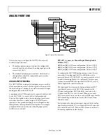
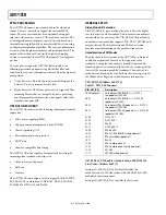
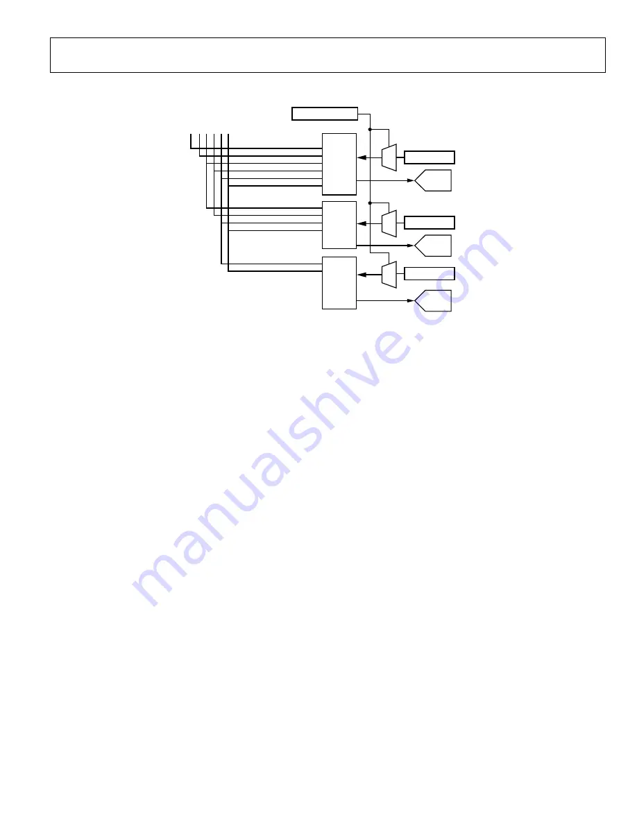
Figure 5. Internal Pin Connections
The two key steps to configure the ADV7181B to correctly
decode the input video are:
•
The analog input muxing section must be configured to
correctly route the video from the analog input pins to the
correct set of ADCs.
•
The standard definition processor block, which decodes
the digital data, should be configured to process either
CVBS, YC, or YPrPb.
ANALOG INPUT MUXING
The ADV7181B has an integrated analog muxing section that
allows more than one source of video signal to be connected to
the decoder. Figure 5 outlines the overall structure of the input
muxing provided in the ADV7181B.
A maximum of six CVBS inputs can be connected and decoded
by the ADV7181B. As seen in the Pin Configuration and
Function Description section, these analog input pins lie near
each other; therefore, a careful design of the PCB layout is
required, such as ground shielding between all signals routed
through tracks that are physically close together. It is strongly
recommended to connect any unused analog input pins to
AGND to act as a shield.
SETADC_sw_man_en, Manual Input Muxing Enable,
Address C4[7]
ADC0_sw[3:0],
ADC0 mux configuration, Address C3[3:0]
ADC1_sw[3:0],
ADC1 mux configuration, Address C3[7:4]
ADC2_sw[3:0],
ADC2 mux configuration, Address C4[3:0]
To configure the ADV7181B analog muxing section, the user
must select the analog input (AIN1 to AIN6) that is to be
processed by each ADC. SETADC_sw_man_en must be set to 1
to enable the muxing blocks to be configured. The three mux
sections are controlled by the signal buses ADC0/1/2_sw[3:0].
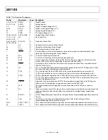
Table 8 explains the control words used.
The input signal that contains the timing information (H/V
syncs) must be processed by ADC0. For example, in the
YC input configuration, ADC0 should be connected to the
Y channel and ADC1 to the C channel. When one or more
ADCs are not used to process video, such as CVBS input, the idle
ADCs should be powered down (see the ADC Power-Down
Control section).
Restrictions on the channel routing are imposed by the analog
signal routing inside the IC; it is not possible for each input pin
to be routed to each ADC. Refer to Table 8 for an overview on
the routing capabilities inside the chip.

