ADV7181B
Rev. B | Page 17 of 100
Enable Subcarrier Frequency Lock Pin
EN_SFL_PIN Address 0x04[1]
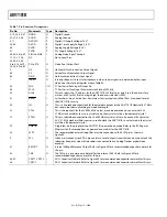
The EN_SFL_PIN bit enables the output of subcarrier lock
information (also known as GenLock) from the ADV7181B
core to an encoder in a decoder-encoder back-to-back
arrangement.
When EN_SFL_PIN is 0 (default), the subcarrier frequency lock
output is disabled.
When EN_SFL_PIN is 1, the subcarrier frequency lock
information is presented on the SFL pin.
Polarity LLC Pin
PCLK Address 0x37[0]
The polarity of the clock that leaves the ADV7181B via the LLC
pin can be inverted using the PCLK bit.
Changing the polarity of the LLC clock output can be necessary
to meet the setup-and-hold time expectations of follow-on
chips.
When PCLK is 0, the LLC output polarity is inverted.
When PCLK is 1 (default), the LLC output polarity is normal
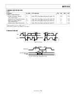
(as per the timing diagrams).

