background image


ADV7181B


Rev. B | Page 23 of 100 

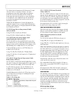
SD_SAT_Cr[7:0] SD Saturation Cr Channel, Address 
0xE4[7:0] 

This register allows the user to control the gain of the Cr 
channel only, which in turn adjusts the saturation of the picture. 

Table 23. SD_SAT_Cr Function 

SD_SAT_Cr[7:0] Description 


0x80 (default) 

Gain on Cr channel = 0 dB 

0x00 

Gain on Cb channel = −42 dB 

0xFF 

Gain on Cb channel = +6 dB 


SD_OFF_Cb[7:0] SD Offset Cb Channel, Address 
0xE1[7:0] 

This register allows the user to select an offset for the Cb 
channel only and adjust the hue of the picture. There is a 
functional overlap with the Hue[7:0] register.  

Table 24. SD_OFF_Cb Function  

SD_OFF_Cb[7:0] Description 

0x80 (default) 

0 offset applied to the Cb channel 

0x00 

−312 mV offset applied to the Cb channel 

0xFF 

+312 mV offset applied to the Cb channel 


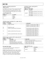
SD_OFF_Cr[7:0] SD Offset Cr Channel, Address 
0xE2[7:0] 

This register allows the user to select an offset for the Cr channel 
only and adjust the hue of the picture. There is a functional 
overlap with the Hue[7:0] register. 

Table 25. SD_OFF_Cr Function 

SD_OFF_Cr[7:0] Description 

0x80 (default) 

0 offset applied to the Cr channel 

0x00 

−312 mV offset applied to the Cr channel 

0xFF 

+312 mV offset applied to the Cr channel 


BRI[7:0] Brightness Adjust, Address 0x0A[7:0] 

This register controls the brightness of the video signal. It 
allows the user to adjust the brightness of the picture. 

Table 26. BRI Function 

BRI[7:0] Description 

0x00 (default) 

Offset of the luma channel = 0IRE 

0x7F 

Offset of the luma channel = +100IRE 

0x80 

Offset of the luma channel = –100IRE 


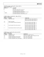
HUE[7:0] Hue Adjust, Address 0x0B[7:0] 

This register contains the value for the color hue adjustment. 
It allows the user to adjust the hue of the picture. 

HUE[7:0] has a range of ±90°, with 0x00 equivalent to an 
adjustment of 0°. The resolution of HUE[7:0] is 1 bit = 0.7°. 

The hue adjustment value is fed into the AM color demodula-
tion block. Therefore, it applies only to video signals that contain 
chroma information in the form of an AM-modulated carrier 
(CVBS or Y/C in PAL or NTSC). It does not affect SECAM and 
does not work on component video inputs (YPrPb). 

Table 27. HUE Function 

HUE[7:0] Description


(Adjust Hue of the Picture) 

0x00 (default) 

Phase of the chroma signal = 0° 

0x7F 

Phase of the chroma signal = –90° 

0x80 

Phase of the chroma signal = +90° 


DEF_Y[5:0] Default Value Y, Address 0x0C[7:2] 

When the ADV7181B loses lock on the incoming video signal 
or when there is no input signal, the DEF_Y[5:0] register allows 
the user to specify a default luma value to be output. This value 
is used under the following conditions: 


If DEF_VAL_AUTO_EN bit is set to high and the 
ADV7181B lost lock to the input video signal. This is 
the intended mode of operation (automatic mode). 


The DEF_VAL_EN bit is set, regardless of the lock 
status of the video decoder. This is a forced mode that 
may be useful during configuration. 

The DEF_Y[5:0] values define the 6 MSBs of the output video. 
The remaining LSBs are padded with 0s. For example, in 8-bit 
mode, the output is Y[7:0] = {DEF_Y[5:0], 0, 0}.  

DEF_Y[5:0] is 0x0D (blue) is the default value for Y. 

Register 0x0C has a default value of 0x36. 

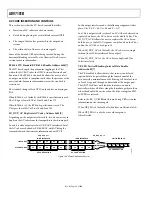
DEF_C[7:0] Default Value C, Address 0x0D[7:0] 

The DEF_C[7:0] register complements the DEF_Y[5:0] value. 
It defines the 4 MSBs of Cr and Cb values to be output if 


The DEF_VAL_AUTO_EN bit is set high and the 
ADV7181B cannot lock to the input video (automatic 
mode). 


DEF_VAL_EN bit is set to high (forced output). 

The data that is finally output from the ADV7181B for the 
chroma side is Cr[7:0] = {DEF_C[7:4], 0, 0, 0, 0}, Cb[7:0] = 
{DEF_C[3:0], 0, 0, 0, 0}. 

DEF_C[7:0] is 0x7C (blue) is the default value for Cr and Cb. 

Summary of Contents for ADV7181B

Page 1: ...CGMS EDTV Gemstar 1 2 VBI decode support for close captioning WSS CGMS EDTV and Gemstar 1 2 Power down mode 2 wire serial MPU interface I2 C compatible 3 3 V analog 1 8 V digital core 3 3 V IO supply...

Page 2: ...cessor SDP 19 SD Luma Path 19 SD Chroma Path 19 Sync Processing 20 VBI Data Recovery 20 General Setup 20 Color Controls 22 Clamp Operation 24 Luma Filter 25 Chroma Filter 28 Gain Operation 29 Chroma T...

Page 3: ...Table 85 72 7 05 Rev 0 to Rev A Changed Crystal References to 28 MHz Crystal Universal Changes to General Description Section 1 Changes to Analog Specifications Section 8 Changes to Clamp Operation Se...

Page 4: ...e of decoding a large selection of baseband video signals in composite S Video and component formats The video standards supported by the ADV7181B include PAL B D I G H PAL60 PAL M PAL N PAL Nc NTSC M...

Page 5: ...LE CHROMA 2D COMB 4H MAX L DNR OUTPUT FORMATTER SYNC EXTRACT LINE LENGTH PREDICTOR RESAMPLE CONTROL AV CODE INSERTION CTI C DNR A D CLAMP 9 9 9 A D CLAMP 9 A D CLAMP 9 VBI DATA RECOVERY GLOBAL CONTROL...

Page 6: ...GITAL OUTPUTS Output High Voltage VOH ISOURCE 0 4 mA 2 4 V Output Low Voltage VOL ISINK 3 2 mA 0 4 V High Impedance Leakage Current ILEAK 10 A Output Capacitance COUT 20 pF POWER REQUIREMENTS3 Digital...

Page 7: ...4 dB Luma flat field 58 dB Analog Front End Crosstalk 60 dB LOCK TIME SPECIFICATIONS Horizontal Lock Range 5 5 Vertical Lock Range 40 70 Hz FSC Subcarrier Lock Range 1 3 kHz Color Lock In Time 60 Line...

Page 8: ...AND CONTROL OUTPUTS Data Output Transitional Time t11 Negative clock edge to start of valid data tACCESS t10 t11 3 4 ns Data Output Transitional Time t12 End of valid data to negative clock edge tHOLD...

Page 9: ...lead LFCSP 9 2 C W Junction to Ambient Thermal Resistance Still Air JA 4 layer PCB with solid ground plane 64 lead LQFP 47 C W Junction to Case Thermal Resistance JC 4 layer PCB with solid ground plan...

Page 10: ...ose listed under Absolute Maximum Ratings may cause permanent damage to the device This is a stress rating only functional operation of the device at these or any other conditions above those indicate...

Page 11: ...REFOUT 41 AVDD 40 CAPY2 39 CAPY1 38 AGND 37 AIN2 36 AIN1 35 DGND 34 NC 33 P4 17 P3 18 P2 19 LLC 20 XTAL1 21 XTAL 22 DVDD 23 DGND 24 P1 25 P0 26 NC 27 NC 28 PWRDN 29 ELPF 30 PVDD 31 AGND 32 VS 64 FIELD...

Page 12: ...he pixel data output by the ADV7181B Nominally 27 MHz but varies up or down according to video line length 22 XTAL I This is the input pin for the 28 6363 MHz crystal or can be overdriven by an extern...

Page 13: ...lding between all signals routed through tracks that are physically close together It is strongly recommended to connect any unused analog input pins to AGND to act as a shield SETADC_sw_man_en Manual...

Page 14: ...n 1010 No connection 1010 No connection 1010 No connection 1011 No connection 1011 No connection 1011 No connection 1100 AIN3 1100 AIN3 1100 No connection 1101 AIN5 1101 AIN5 1101 AIN5 1110 No connect...

Page 15: ...DCs should be powered down when in CVBS mode ADC 1 and ADC 2 should be powered down to save on power consumption S Video mode ADC 2 should be powered down to save on power consumption PWRDN_ADC_0 Addr...

Page 16: ...in free run mode where a separate chip can output for instance a company logo For more information on three state control see the Three State Output Drivers and the Three State LLC Driver sections Ind...

Page 17: ...cy lock output is disabled When EN_SFL_PIN is 1 the subcarrier frequency lock information is presented on the SFL pin Polarity LLC Pin PCLK Address 0x37 0 The polarity of the clock that leaves the ADV...

Page 18: ...D_RESULT Function AD_RESULT 2 0 Description 000 NTSM MJ 001 NTSC 443 010 PAL M 011 PAL 60 100 PAL B G H I D 101 SECAM 110 PAL Combination N 111 SECAM 525 Table 14 STATUS 1 Function STATUS 1 7 0 Bit Na...

Page 19: ...al gain Luma Resample To correct for line length errors as well as dynamic line length changes the data is digitally resampled Luma 2D Comb The two dimensional comb filter provides YC separation AV Co...

Page 20: ...n configure itself to support PAL B G H I D PAL M N PAL combination N NTSC M NTSC J SECAM 50 Hz 60 Hz NTSC4 43 and PAL60 GENERAL SETUP Video Standard Selection The VID_SEL 3 0 register allows the user...

Page 21: ...ed to solve some compatibility issues with video encoders It solves two problems First the PAL switch bit is only meaningful in PAL Some encoders including Analog Devices encoders also look at the sta...

Page 22: ...unt Into Lock Address 0x51 2 0 CIL 2 0 determines the number of consecutive lines for which the lock condition must be true before the system switches into the locked state and reports this via Status...

Page 23: ...UE 7 0 has a range of 90 with 0x00 equivalent to an adjustment of 0 The resolution of HUE 7 0 is 1 bit 0 7 The hue adjustment value is fed into the AM color demodula tion block Therefore it applies on...

Page 24: ...e clamping can be divided into two sections Clamping before the ADC analog domain current sources Clamping after the ADC digital domain digital processing block The ADCs can digitize an input signal o...

Page 25: ...ault the digital clamp is operational When DCFE is 1 the digital clamp loop is frozen LUMA FILTER Data from the digital fine clamp block is processed by three sets of filters The data format at this p...

Page 26: ...aping filter mode for good quality CVBS component YPrPb and S VHS YC input signals In automatic mode the system preserves the maximum possible bandwidth for good CVBS sources since they can successful...

Page 27: ...011 SVHS 18 CCIR 601 1 0100 PAL NN 1 1 0101 PAL NN 2 1 0110 PAL NN 3 1 0111 PAL WN 1 1 1000 PAL WN 2 1 1001 NTSC NN 1 1 1010 NTSC NN 2 1 1011 NTSC NN 3 1 1100 NTSC WN 1 1 1101 NTSC WN 2 1 1110 NTSC WN...

Page 28: ...4 Figure 14 NTSC Notch Filter Response CHROMA FILTER Data from the digital fine clamp block is processed by three sets of filters The data format at this point is CVBS for CVBS inputs chroma only for...

Page 29: ...ong as it fits into the ADC window The components to this are the amplitude of the input signal and the dc level it resides on The dc level is set by the clamping circuitry see the Clamp Operation sec...

Page 30: ...n control This register only has an effect if the LAGC 2 0 register is set to 001 010 011 or 100 automatic gain control modes If peak white AGC is enabled and active see the STATUS_1 7 0 Address 0x10...

Page 31: ...out pedestal selects BETACAM variant Selecting NTSC with pedestal selects BETACAM Selecting NTSC without pedestal selects BETACAM variant PW_UPD Peak White Update Address 0x2B 0 The peak white and ave...

Page 32: ...tion works only for input signals with a modulated chroma part For component input YPrPb there is no color kill Setting CKE to 0 disables color kill Setting CKE to 1 default enables color kill CKILLTH...

Page 33: ...mooth mixing 11 default Smoothest alpha blend function CTI_C_TH 7 0 CTI Chroma Threshold Address 0x4E 7 0 The CTI_C_TH 7 0 value is an unsigned 8 bit number speci fying how big the amplitude step in a...

Page 34: ...line memory Fixed 4 line chroma comb for CTAPSN 11 Fixed 3 line chroma comb for CTAPSN 01 Fixed 4 line chroma comb for CTAPSN 10 110 Fixed chroma comb all lines of line memory Fixed 5 line chroma comb...

Page 35: ...CTAPSP 01 Fixed 3 line chroma comb for CTAPSP 10 101 Fixed chroma comb top lines of line memory Fixed 4 line chroma comb for CTAPSP 11 Fixed 3 line chroma comb for CTAPSP 01 Fixed 4 line chroma comb f...

Page 36: ...ransmitted word that contains information about H V F In this output interface mode the following assignment takes place Cb FF Y 00 Cr 00 and Y AV In a 16 bit output interface where Y and Cr Cb are de...

Page 37: ...UTO_PDC_EN bit to 0 the values programmed into LTA 1 0 and CTA 2 0 registers become active When AUTO_PDC_EN is 0 the ADV7181B uses the LTA 1 0 and CTA 2 0 values for delaying luma and chroma samples R...

Page 38: ...igure 19 HSE is set to 00000000000b which is 0 LLC1 clock cycles from Count 0 The default value of HSE 10 0 is 000 indicating that the HS pulse ends zero pixels after a falling edge of HS For example...

Page 39: ...e bit in the AV code becomes active Some follow on chips require the VS pin to only change state when HS is high low When VSBHO is 0 default the VS pin goes high at the middle of a line of video odd f...

Page 40: ...7 1 1BT 656 4 REG 0x04 BIT 7 1 1APPLIES IF NEWAVMODE 0 MUST BE MANUALLY SHIFTED IF NEWAVMODE 1 262 263 264 265 266 267 268 269 270 271 272 273 274 275 276 283 284 285 04984 020 Figure 20 NTSC Default...

Page 41: ...84 022 Figure 22 NTSC Vsync Begin NVBEGDELO NTSC Vsync Begin Delay on Odd Field Address 0xE5 7 When NVBEGDELO is 0 default there is no delay Setting NVBEGDELO to 1 delays Vsync going high on an odd fi...

Page 42: ...n an even field by a line relative to NVEND NVENDSIGN NTSC Vsync End Sign Address 0xE6 5 Setting NVENDSIGN to 0 default delays the end of Vsync Set for user manual programming Setting NVENDSIGN to 1 a...

Page 43: ...ntrol 3 0x84 0x34 Hsync Pos Control 1 0x00 0x35 Hsync Pos Control 2 0x00 0x36 Hsync Pos Control 3 0x7D 0x37 Polarity 0xA1 0xE8 PAL_V_Bit_Beg 0x41 0xE9 PAL_V_Bit_End 0x84 0xEA PAL_F_Bit_Tog 0x06 NFTOGS...

Page 44: ...04984 025 Figure 25 PAL Default BT 656 The Polarity of H V and F is Embedded in the Data FIELD 1 622 623 624 625 1 2 3 4 5 6 7 8 9 10 11 23 24 310 311 312 313 314 315 316 317 318 319 320 321 322 323 3...

Page 45: ...er programming PVBEG 4 0 PAL Vsync Begin Address 0xE8 4 0 The default value of PVBEG is 00101 indicating the PAL Vsync begin position For all NTSC PAL Vsync timing controls both the V bit in the AV co...

Page 46: ...he blocks can be disabled via the following two I2 C bits ENHSPLL Enable Hsync Processor Address 0x01 6 The Hsync processor is designed to filter incoming Hsyncs that have been corrupted by noise prov...

Page 47: ...uence is detected Confidence in decoded data is high CGMSD CGMS A Sequence Detected Address 0x90 3 Logic 1 for this bit indicates the data in the CGMS1 2 3 registers is valid The CGMSD bit goes high i...

Page 48: ...ess 0x96 7 0 CGMS2 7 0 Address 0x97 7 0 CGMS3 7 0 Address 0x98 7 0 Figure 32 shows the bit correspondence between the analog video waveform and the CGMS1 CGMS2 CGMS3 registers CGMS3 7 4 are undetermin...

Page 49: ...and a decision is made as to whether or not a particular line is black The threshold value needed can depend on the type of input signal some control is provided via LB_TH 4 0 Detection at the Start...

Page 50: ...fields GDECAD configures the way in which data is embedded in the video data stream The recovered data is not available through I2 C but is inserted into the horizontal blanking period of an ITU R BT...

Page 51: ...entification value is 0x140 10 bit value Care has been taken so the two LSBs do not carry vital information in 8 bit systems EP and EP The EP bit is set to ensure even parity on the data word D 8 0 Ev...

Page 52: ...Mode Byte D 9 D 8 D 7 D 6 D 5 D 4 D 3 D 2 D 1 D 0 Description 0 0 0 0 0 0 0 0 0 0 0 Fixed preamble 1 1 1 1 1 1 1 1 1 1 1 Fixed preamble 2 1 1 1 1 1 1 1 1 1 1 Fixed preamble 3 0 1 0 1 0 0 0 0 0 0 DID...

Page 53: ...1 1 1 1 1 1 1 1 Fixed preamble 2 1 1 1 1 1 1 1 1 1 1 Fixed preamble 3 0 1 0 1 0 0 0 0 0 0 DID 4 EP EP EF 0 Line 3 0 0 0 SDID 5 EP EP 0 0 0 0 0 1 0 0 Data count 6 Gemstar Word1 7 0 0 0 User data words...

Page 54: ...x48 7 0 Address 0x49 7 0 and the GDECOL 15 0 Gemstar Decoding Odd Lines Address 0x4A 7 0 Address 0x4B 7 0 sections Table 70 NTSC CCAP Data Full Byte Mode Byte D 9 D 8 D 7 D 6 D 5 D 4 D 3 D 2 D 1 D 0 D...

Page 55: ...CCAP data from any line in the even field GDECOL 15 0 Gemstar Decoding Odd Lines Address 0x4A 7 0 Address 0x4B 7 0 The 16 bits of the GDECOL 15 0 form a collection of 16 individual line decode enable...

Page 56: ...CEL 12 Gemstar 13 286 23 GDECEL 13 Gemstar 14 287 24 GDECEL 14 Gemstar 15 288 25 GDECEL 15 Gemstar Table 74 PAL Line Enable Bits and Corresponding Line Numbering Line 3 0 Line Number ITU R BT 470 Enab...

Page 57: ...PAGE 1 ADDRESS 0x40 0xFF NORMAL REGISTER SPACE I2C SPACE REGISTER ACCESS PAGE 2 ADDRESS 0x40 0x4C INTERRUPT REGISTER SPACE 04984 037 Figure 37 Register Access Page 1 and Page 2 Interrupt Request Outpu...

Page 58: ...the ADV7181B does not generate a second interrupt signal The system controller should check all unmasked interrupt status bits since more than one can be active Macrovision Interrupt Selection Bits Th...

Page 59: ...When SWPC is 0 default no swapping is allowed When SWPC is 1 the Cr and Cb values can be swapped LLC1 Output Selection LLC_PAD_SEL 2 0 Address 0x8F 6 4 The following I2 C write allows the user to sel...

Page 60: ...on the LSB of the first byte means that the master reads information from the peripheral The ADV7181B acts as a standard slave device on the bus The data on the SDA pin is eight bits long supporting t...

Page 61: ...SR to SR0 These bits are set up to point to the required starting address I2 C SEQUENCER An I2 C sequencer is used when a parameter exceeds eight bits and is therefore distributed over two or more I2...

Page 62: ...xx xxxx rw 22 0x16 Shaping Filter Control 0000 0001 rw 23 0x17 Shaping Filter Control 2 1001 0011 rw 24 0x18 Comb Filter Control 1111 0001 rw 25 0x19 Reserved xxxx xxxx rw 26 to 28 0x1A to 0x1C ADI Co...

Page 63: ...50 0x96 CGMS 2 xxxx xxxx r 151 0x97 CGMS 3 xxxx xxxx r 152 0x98 CCAP 1 xxxx xxxx r 153 0x99 CCAP 2 xxxx xxxx r 154 0x9A Letterbox 1 xxxx xxxx r 155 0x9B Letterbox 2 xxxx xxxx r 156 0x9C Letterbox 3 xx...

Page 64: ...1 DEF_Y 0 DEF_VAL_ AUTO_EN DEF_VAL_EN Default Value C DEF_C 7 DEF_C 6 DEF_C 5 DEF_C 4 DEF_C 3 DEF_C 2 DEF_C 1 DEF_C 0 ADI Control SUB_USR_EN 0 Power Management RES PWRDN PDBP Status 1 COL_KILL AD_RESU...

Page 65: ...6 CTI_C_TH 5 CTI_C_TH 4 CTI_C_TH 3 CTI_C_TH 2 CTI_C_TH 1 CTI_C_TH 0 Reserved CTI DNR Ctrl 4 DNR_TH 7 DNR_TH 6 DNR_TH 5 DNR_TH 4 DNR_TH 3 DNR_TH 2 DNR_TH 1 DNR_TH 0 Lock Count FSCLE SRLS COL 2 COL 1 CO...

Page 66: ...D_SAT_CR 5 SD_SAT_CR 4 SD_SAT_CR 3 SD_SAT_CR 2 SD_SAT_CR 1 SD_SAT_CR 0 NTSC V Bit Begin NVBEGDEL O NVBEGDEL E NVBEGSIGN NVBEG 4 NVBEG 3 NVBEG 2 NVBEG 1 NVBEG 0 NTSC V Bit End NVENDDEL O NVENDDEL E NVE...

Page 67: ...0 0x46 MPU_ STIM_ INTRQ_Q WSS_ CHNGD_Q CGMS_ CHNGD_Q GEMD_Q CCAPD_Q Interrupt Clear 2 0xxx 0000 w 71 0x47 MPU_ STIM_INT RQ_CLR WSS_ CHNGD_ CLR CGMS_ CHNGD_ CLR GEMD_ CLR CCAPD_ CLR Interrupt Maskb 2 0...

Page 68: ...LOCK_Q 1 SD input has caused the decoder to go from an unlocked state to a locked state 0 No change SD_UNLOCK_Q 1 SD input has caused the decoder to go from a locked state to an unlocked state Reserve...

Page 69: ...he input video signal 0 No change detected in CGMS data in the input video signal CGMS_CHNGD_Q 1 A change is detected in the CGMS data in the input video signal 0 No change detected in WSS data in the...

Page 70: ...Reserved x Not used Reserved x Not used 0x49 Raw Status 3 Read Only Register Register Access Page 2 Reserved x Not used These bits cannot be cleared or masked Register 0x4A is used for this purpose 0...

Page 71: ...t Reserved x Not used 0x4B Interrupt Clear 3 Write Only Register Register Access Page 2 Reserved x Not used 0 Masks SD_OP_CHNG_Q bit SD_OP_CHNG_MSKB 1 Unmasks SD_OP_CHNG_Q bit 0 Masks SD_V_LOCK_CHNG_Q...

Page 72: ...PAL B G H I D NTSC M with pedestal SECAM 0 0 1 0 Autodetect PAL N NTSC M without pedestal SECAM 0 0 1 1 Autodetect PAL N NTSC M with pedestal SECAM 0 1 0 0 NTSC J 0 1 0 1 NTSC M 0 1 1 0 PAL60 0 1 1 1...

Page 73: ...19 0 HS VS FIELD and SFL 1 Drivers three stated 0 All lines filtered and scaled 0x03 Output Control VBI_EN Allows VBI data Lines 1 to 21 to be passed through with only a minimum amount of filtering pe...

Page 74: ...0IRE 0x7F 100IRE 0x80 100IRE 0x0B Hue Register HUE 7 0 This register contains the value for the color hue adjustment 0 0 0 0 0 0 0 0 Hue range 90 to 90 0x0C Default Value Y 0 Free run mode dependent o...

Page 75: ...0 1 0 0 PAL B G H I D 1 0 1 SECAM 1 1 0 PAL combination N AD_RESULT 2 0 Autodetection result reports the standard of the input video 1 1 1 SECAM 525 Detected standard COL_KILL x Color kill is active 1...

Page 76: ...SVHS 6 0 1 0 0 0 SVHS 7 0 1 0 0 1 SVHS 8 0 1 0 1 0 SVHS 9 0 1 0 1 1 SVHS 10 0 1 1 0 0 SVHS 11 0 1 1 0 1 SVHS 12 0 1 1 1 0 SVHS 13 0 1 1 1 1 SVHS 14 1 0 0 0 0 SVHS 15 1 0 0 0 1 SVHS 16 1 0 0 1 0 SVHS...

Page 77: ...used for the Y component of Y C YPbPr B W input signals it is also used when a good quality input CVBS signal is detected For all other inputs the Y shaping filter chosen is controlled by YSFM 4 0 1 1...

Page 78: ...Swap the Cr and Cb O P samples See Swap_CR_CB_WB Addr 0x89 0x2B 0 Update once per video line PW_UPD Peak white update determines the rate of gain 1 Update once per field Peak white must be enabled See...

Page 79: ...ffect only if LAGC 1 0 is set to auto gain 001 010 011 or 100 0x30 Luma Gain Control 2 LMG 7 0 Luma manual gain can be used to program a desired manual chroma gain or read back the actual used gain va...

Page 80: ...0 Active high PF Sets the FIELD polarity 1 Active low Reserved 0 Set to 0 0 Active high PVS Sets the VS Polarity 1 Active low Reserved 0 Set to 0 0 Active high 0x37 Polarity PHS Sets the HS Polarity...

Page 81: ...ttom lines of memory Fixed 3 line for CTAPSN 10 CCMP 2 0 Chroma comb mode PAL 1 1 1 Fixed 4 line for CTAPSN 11 0 0 Not used 0 1 Adapts 5 lines 3 lines 2 taps 1 0 Adapts 5 lines 3 lines 3 taps PAL Comb...

Page 82: ...that the decoder checks for Gemstar compatible data LSB Line 10 MSB Line 25 Default Do not check for Gemstar compatible data on any lines 10 to 25 in odd fields 0 Split data into half byte To avoid 00...

Page 83: ...minal 27 MHz selected out on LLC1 pin LLC_PAD_SEL 2 0 Enables manual selection of clock for LLC1 pin 1 0 1 LLC2 nominally 13 5 MHz selected out on LLC1 pin For 16 bit 4 2 2 out OF_SEL 3 0 0010 0x8F Fr...

Page 84: ...ach field It enables format detection even if the video is not accompanied by a CGMS or WSS sequence Reserved 0 0 Set as default 0 Turn off CRC check CRC_ENABLE Enable CRC checksum decoded from CGMS p...

Page 85: ...ol 2 LB_SL 3 0 Program the start line of the activity window for LB detection start of field 0 1 0 0 Letterbox detection aligned with the start of active video 0100b 23 286 NTSC 0xDE Reserved 0 0 0 0...

Page 86: ...0 0 1 0 1 PAL default BT 656 0 Set to low when manual programming PVBEGSIGN 1 Not suitable for user programming 0 No delay PVBEGDELE Delay V bit going high by one line relative to PVBEG even field 1 A...

Page 87: ...sed or decreased for EMC or crosstalk reasons 1 1 High drive strength 4x 0xF4 Drive Strength Reserved x x No delay 0 0 0 Bypass mode 0 dB 2 MHz 5 MHz 0 0 1 3 dB 2 dB 0 1 0 6 dB 3 5 dB 0 1 1 10 dB 5 dB...

Page 88: ...e manual muxing 0x0E 0x80 ADI recommended programming sequence This sequence must be followed exactly when setting up the decoder 0x50 0x20 Recommended setting 0x52 0x18 Recommended setting 0x58 0xED...

Page 89: ...0x80 ADI recommended programming sequence This sequence must be followed exactly when setting up the decoder 0x50 0x20 Recommended setting 0x52 0x18 Recommended setting 0x58 0xED Recommended setting 0...

Page 90: ...l muxing Man mux AIN5 to ADC2 1101 0x0E 0x80 ADI recommended programming sequence This sequence must be followed exactly when setting up the decoder 0x52 0x18 Recommended setting 0x58 0xED Recommended...

Page 91: ...ual mux AIN6 to ADC0 0101 0xC4 0x80 Enable manual muxing 0x0E 0x80 ADI recommended programming sequence This sequence must be followed exactly when setting up the decoder 0x50 0x20 Recommended setting...

Page 92: ...ting 0xE4 0x3E Recommended setting 0xEA 0x0F Recommended setting 0xE9 0x3E Recommended setting 0x0E 0x00 Recommended setting Mode 2 S Video Input Y on AIN1 and C on AIN4 All standards are supported th...

Page 93: ...nual mux AIN1 to ADC0 1001 AIN3 to ADC1 1100 0xC4 0x8D Enable manual muxing manual mux AIN5 to ADC2 1101 0x0E 0x80 ADI recommended programming sequence This sequence must be followed exactly when sett...

Page 94: ...down ADC 1 and ADC 2 0x50 0x0A Set higher DNR threshold 0xC3 0x05 Manual mux AIN6 to ADC0 0101 0xC4 0x80 Enable manual muxing 0x0E 0x80 ADI recommended programming sequence This sequence must be follo...

Page 95: ...ast PVDD from a different cleaner power source for example from a 12 V supply It is also recommended to use a single ground plane for the entire board This ground plane should have a space between the...

Page 96: ...t These clamps ensure the video stays within the 5 V range of the op amp used 0 20 40 60 80 100 120 100k 30M 10M 3M 1M 300k 300M 1G 100M FREQUENCY Hz 04984 042 Figure 42 Third Order Butterworth Filter...

Page 97: ...n Figure 44 and Figure 45 For a detailed schematic diagram for the ADV7181B refer to the ADV7181B evaluation note B Q6 C E R38 75 R89 5 6k R63 820 R43 0 R53 56 R24 470 R39 4 7k C95 22pF C102 10pF C93...

Page 98: ...O P ELPF 1 69k 10nF 82nF PVDD DGND DVDDIO 100nF P0 P1 P2 P3 P4 P5 P6 P7 P8 P9 P10 P11 P12 P13 P14 P15 MULTI FORMAT PIXEL PORT 10 F 0 1 F REFOUT AGND 0 1 F 10 F XTAL 47pF DGND XTAL1 ALSB 47pF DGND 28...

Page 99: ...HE BOTTOM OF THE LFCSP PACKAGE MUST BE SOLDERED TO PCB GROUND FOR PROPER HEAT DISSIPATION AND ALSO FOR NOISE AND MECHANICAL STRENGTH BENEFITS Figure 46 64 Lead Lead Frame Chip Scale Package LFCSP_VQ 9...

Page 100: ...n withstand surface mount soldering at up to 255 C 5 C In addition it is backward compatible with conventional SnPb soldering processes This means the electroplated Sn coating can be soldered with Sn...

Reviews: