ADV7181B
Rev. B | Page 48 of 100
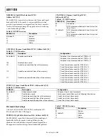
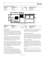
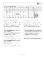
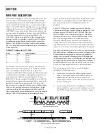
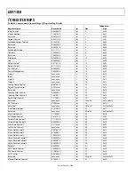
Table 57. WSS Access Information
Signal Name
Register Location
Address
Register Default Value
WSS1[7:0]
WSS 1[7:0]
145d
0x91
Readback only
WSS2[5:0]
WSS 2[5:0]
146d
0x92
Readback only
EDTV1[7:0]
EDTV2[7:0]
EDTV3[5:0]
NOT SUPPORTED
0
1
3
4
5
6
7
0
1
2 3 4
5
6
7
0
1
2
3
4
5
2
04984-031
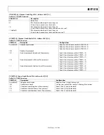
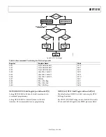
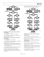
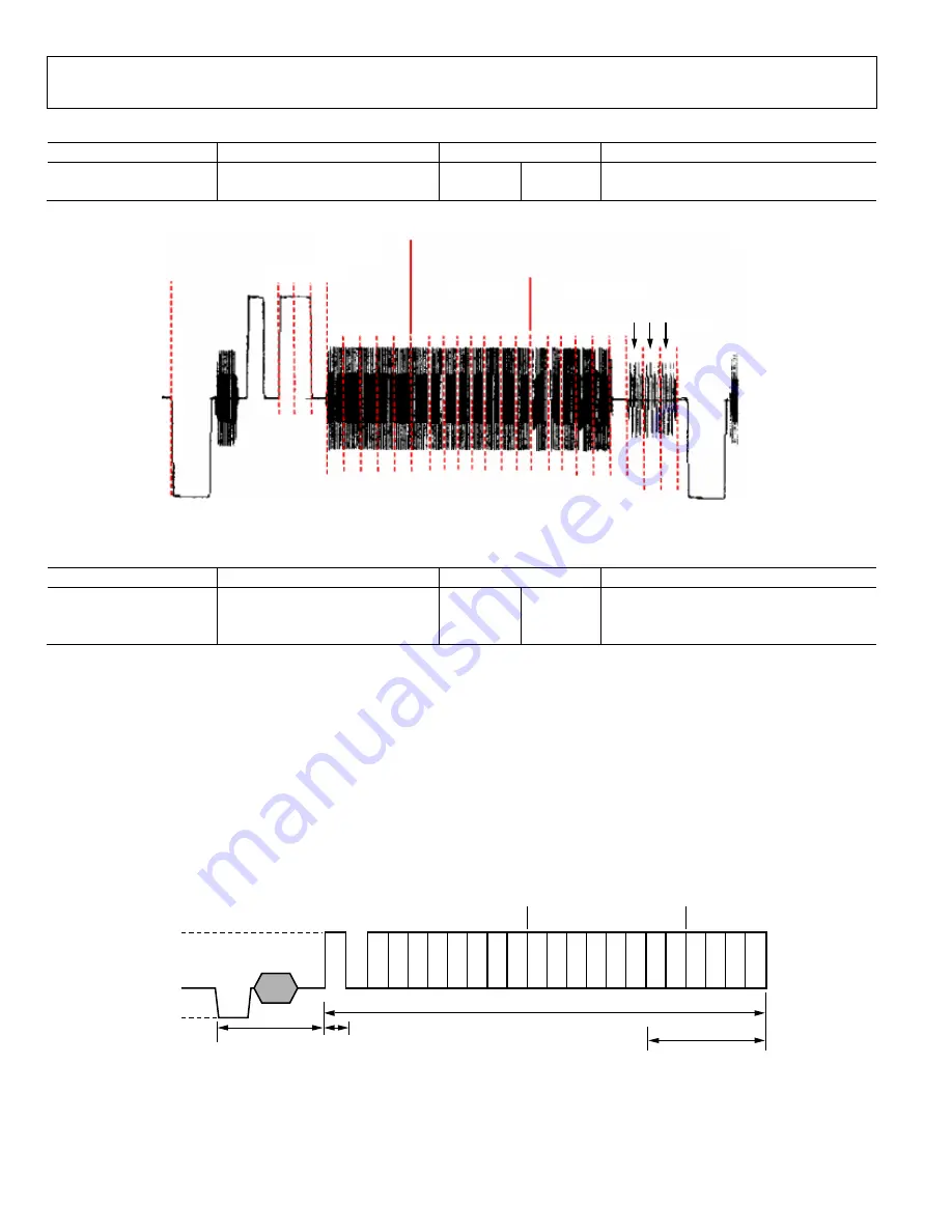
Figure 31. EDTV Data Extraction
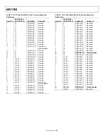
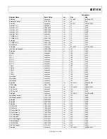
Table 58. EDTV Access Information
Signal Name
Register Location
Address
Register Default Value
EDTV1[7:0]
EDTV 1[7:0]
147d
0x93
Readback only
EDTV2[7:0]
EDTV 2[7:0]
148d
0x94
Readback only
EDTV3[7:0]
EDTV 3[7:0]
149d
0x95
Readback only
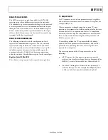
CGMS Data Registers
CGMS1[7:0], Address 0x96[7:0]
CGMS2[7:0], Address 0x97[7:0]
CGMS3[7:0], Address 0x98[7:0]
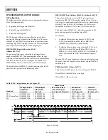
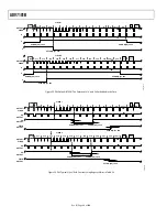
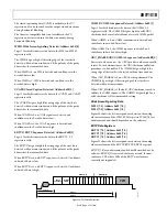
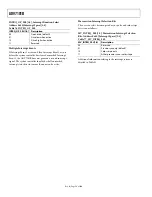
Figure 32 shows the bit correspondence between the analog
video waveform and the CGMS1/CGMS2/CGMS3 registers.
CGMS3[7:4] are undetermined and should be masked out by
software.
Closed Caption Data Registers
CCAP1[7:0], Address 0x99[7:0]
CCAP2[7:0], Address 0x9A[7:0]
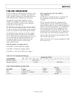
Figure 33 shows the bit correspondence between the analog
video waveform and the CCAP1/CCAP2 registers.
CCAP1[7] contains the parity bit from the first word.
CCAP2[7] contains the parity bit from the second word.
Refer to the GDECAD Gemstar Decode Ancillary Data Format,
Address 0x4C[0] section.
0
1
2
3
4
5
6
7
0
1
2
3
4
5
6
7
0
1
2
3
CGMS2[7:0]
CGMS3[3:0]
CGMS1[7:0]
REF
+100 IRE
+70 IRE
0 IRE
–40 IRE
11.2
μ
s
49.1
μ
s
±
0.5
μ
s
CRC SEQUENCE
2.235
μ
s
±
20ns
04984-032
Figure 32. CGMS Data Extraction

