ADV7181B
Rev. B | Page 6 of 100
SPECIFICATIONS
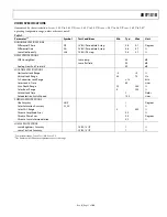
ELECTRICAL CHARACTERISTICS
A
VDD
= 3.15 V to 3.45 V, D
VDD
= 1.65 V to 2.0 V, D
VDDIO
= 3.0 V to 3.6 V, P
VDD
= 1.65 V to 2.0 V; operating temperature range, unless
otherwise noted.
Table 1.
Parameter
1, 2
Symbol
Test
Conditions
Min
Typ
Max
Unit
STATIC PERFORMANCE
Resolution (Each ADC)
N
9
Bits
Integral Nonlinearity
INL
BSL at 54 MHz
−0.475/+0.6
−1.5/+2
LSB
Differential Nonlinearity
DNL
BSL at 54 MHz
–0.25/+0.5
–0.7/+2
LSB
DIGITAL INPUTS
Input High Voltage
V
IH
2
V
Input Low Voltage
V
IL
0.8 V
Input Current
I
IN
Pin
29
–50
+50
μA
All other pins
–10
+10
μA
Input Capacitance
C
IN
10 pF
DIGITAL OUTPUTS
Output High Voltage
V
OH
I
SOURCE
= 0.4 mA
2.4
V
Output Low Voltage
V
OL
I
SINK
= 3.2 mA
0.4
V
High Impedance Leakage Current
I
LEAK
10 μA
Output Capacitance
C
OUT
20 pF
POWER REQUIREMENTS
3
Digital Core Power Supply
D
VDD
1.65
1.8
2
V
Digital I/O Power Supply
D
VDDIO
3.0
3.3
3.6
V
PLL Power Supply
P
VDD
1.65
1.8
2.0 V
Analog Power Supply
A
VDD
3.15
3.3
3.45 V
Digital Core Supply Current
I
DVDD
80
mA
Digital I/O Supply Current
I
DVDDIO
2
mA
PLL Supply Current
I
PVDD
10.5
mA
Analog Supply Current
I
AVDD
CVBS
input
4
85 mA
YPrPb
input
5
180 mA
Power-Down Current
I
PWRDN
1.5
mA
Power-Up Time
t
PWRUP
20
ms
1
Temperature range: T
MIN
to T
MAX
, –40°C to +85°C.
2
The min/max specifications are guaranteed over this range.
3
Guaranteed by characterization.
4
ADC1 and ADC2 powered down.
5
All three ADCs powered on.

