ADV7181B
Rev. B | Page 96 of 100
DIGITAL INPUTS
The digital inputs on the ADV7181B are designed to work with
3.3 V signals, and are not tolerant of 5 V signals. Extra compo-
nents are needed if 5 V logic signals are required to be applied
to the decoder.
ANTIALIASING FILTERS
For inputs from some video sources that are not bandwidth
limited, signals outside the video band can alias back into the
video band during A/D conversion and appear as noise on the
output video. The ADV7181B oversamples the analog inputs by
a factor of 4. This 54 MHz sampling frequency reduces the
requirement for an input filter; for optimal performance it is
recommended an antialiasing filter be used. The recommended
low-cost circuit for implementing this buffer and filter circuit
for all analog input signals is shown in Figure 44.
The buffer is a simple emitter-follower using a single npn
transistor. The antialiasing filter is implemented using passive
components. The passive filter is a third-order Butterworth
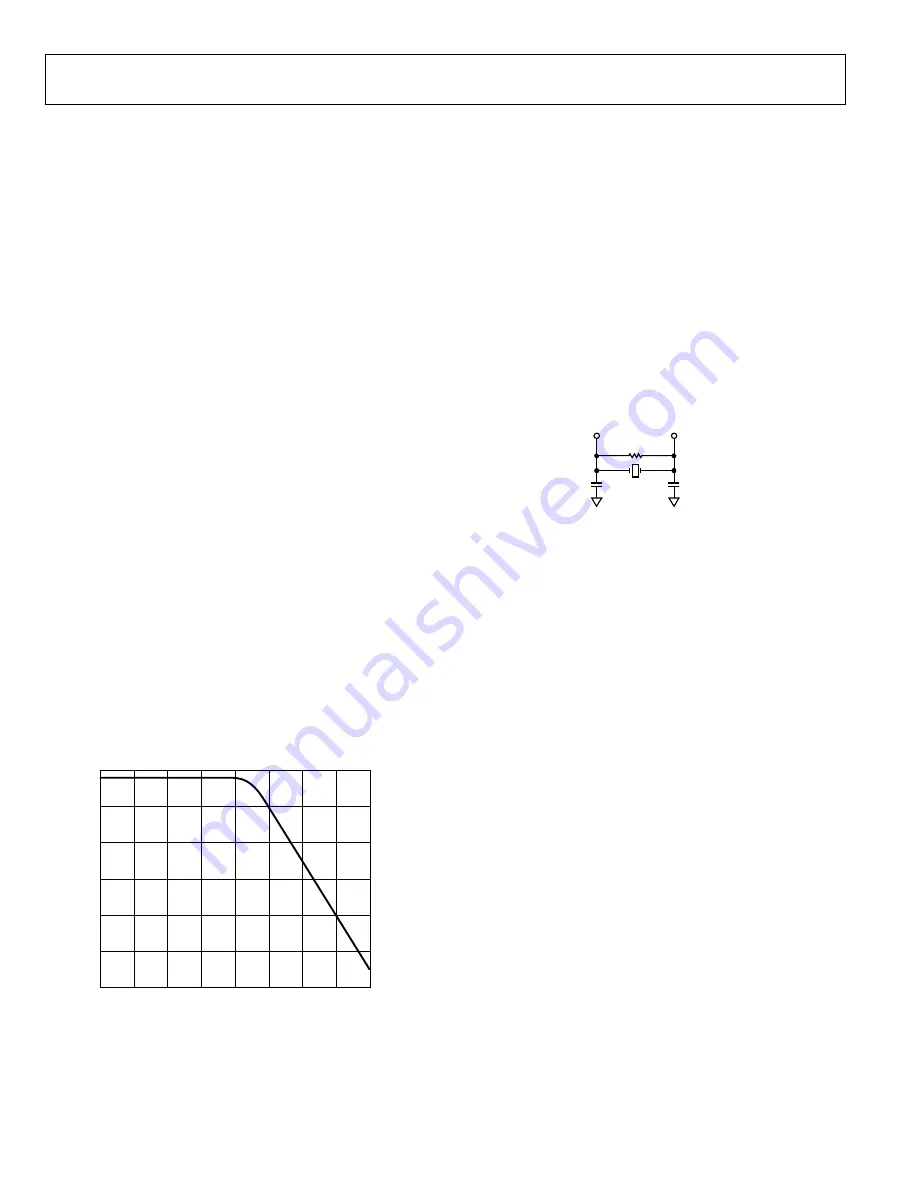
filter with a −3 dB point of 9 MHz. The frequency response of
the passive filter is shown in Figure 42. The flat pass band up to
6 MHz is essential. The attenuation of the signal at the output of
the filter due to the voltage divider of R24 and R63 is compen-
sated for in the ADV7181B part using the automatic gain control.
The ac-coupling capacitor at the input to the buffer creates a
high-pass filter with the biasing resistors for the transistor. This
filter has a cut-off of
{2 × π × (
R
39||
R
89) ×
C
93}
–1
= 0.62 Hz
It is essential the cutoff of this filter be less than 1 Hz to ensure
correct operation of the internal clamps within the part. These
clamps ensure the video stays within the 5 V range of the
op amp used.
0
–20
–40
–60
–80
–100
–120
100k
30M
10M
3M
1M
300k
300M
1G
100M
FREQUENCY (Hz)
04984-042
Figure 42. Third-Order Butterworth Filter Response
CRYSTAL LOAD CAPACITOR VALUE SELECTION
Figure 43 shows an example reference clock circuit for the a
ADV7181B. Special care must be taken when using a crystal
circuit to generate the reference clock for the ADV7181B. Small
variations in reference clock frequency can cause autodetection
issues and impair the ADV7181B performance.
Load capacitor values are dependant on crystal attributes.
The load capacitance given in a crystal data sheet specifies the
parallel resonance frequency within the tolerance at 25
°
C. It is
therefore important to design a circuit that matches the load
capacitance in order to achieve the frequency stipulated by the
manufacturer. For detailed crystal circuit design and optimiza-
tion, an applications note on crystal design considerations is
available for reference.
C1
47pF
C2
47pF
R = 1M
Ω
XTAL
28.63636MHz
04984-046
XTAL
XTAL 1
Figure 43. Crystal Circuit
Use the following guidelines to ensure correct operation:
•
Use the correct frequency crystal, which is 28.63636 MHz.
Tolerance should be 50 ppm or better.
•
Use a parallel-resonant crystal.
•
Place a 1 MΩ shunt resistor across pins XTAL1 and
XTAL2 as is shown in Figure 43.
•
Know the C
LOAD
for the crystal part number selected. The
value of Capacitors C1 and C2 must match C
LOAD
for the
specific crystal part number in the user’s system.
To determine C
LOAD
, use the following guideline:
C
1 =
C
2 =
C
C
= 2 ( C
LOAD
–
C
s
) -
C
pg
where:
C
pg
is the pin-to-ground capacitance; approximately
4 pF to 10 pF.
C
S
is the PCB stray capacitance, approximately
2 pF to-3 pF.
For example,
C
LOAD
= 30 pF
C = 2 ( 30-3 ) − 4
= 50 pF
Therefore, two 47 pF capacitors can be chosen for
C1 and C2.

