ADV7181B
Rev. B | Page 97 of 100
TYPICAL CIRCUIT CONNECTION
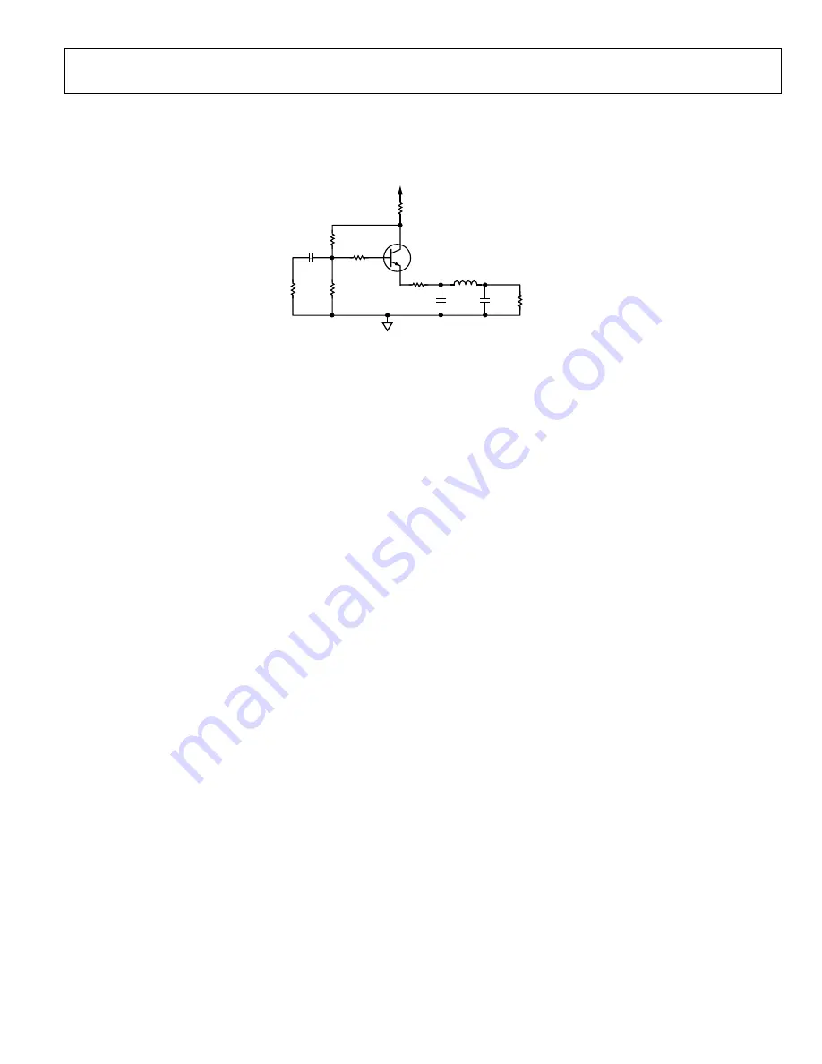
Examples of how to connect the ADV7181B video decoder are shown in Figure 44 and Figure 45. For a detailed schematic diagram for
the ADV7181B, refer to the ADV7181B evaluation note.
B
Q6
C
E
R38
75
Ω
R89
5.6k
Ω
R63
820
Ω
R43
0
Ω
R53
56
Ω
R24
470
Ω
R39
4.7k
Ω
C95
22pF
C102
10pF
C93
100
μ
F
AVDD_5V
L10
12
μ
H
FILTER
BUFFER
AGND
04984-043
Figure 44. ADI Recommended Antialiasing Circuit for All Input Channels


