ADV7181B
Rev. B | Page 46 of 100
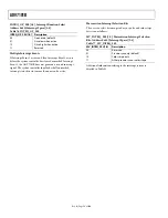
PVEND[4:0] PAL Vsync End, Address 0xE9[4:0]
The default value of PVEND is 10100, indicating the PAL Vsync
end position.
For all NTSC/PAL Vsync timing controls, both the V bit in the
AV code and the Vsync on the VS pin are modified.
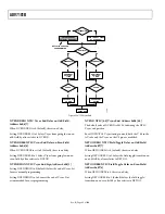
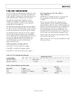
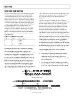
PFTOGDELO PAL Field Toggle Delay on Odd Field,
Address 0xEA[7]
When PFTOGDELO is 0 (default), there is no delay.
Setting PFTOGDELO to 1 delays the F toggle/transition on an
odd field by a line relative to PFTOG.
PFTOGDELE PAL Field Toggle Delay on Even Field,
Address 0xEA[6]
When PFTOGDELE is 0, there is no delay.
Setting PFTOGDELE to 1 (default) delays the F toggle/
transition on an even field by a line relative to PFTOG.
PFTOGSIGN PAL Field Toggle Sign, Address 0xEA[5]
Setting PFTOGSIGN to 0 delays the field transition. Set for user
manual programming.
Setting PFTOGSIGN to 1 (default) advances the field transition.
Not recommended for user programming.
PFTOG PAL Field Toggle, Address 0xEA[4:0]
The default value of PFTOG is 00011, indicating the PAL field
toggle position.
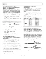
For all NTSC/PAL Field timing controls, the F bit in the AV
code and the field signal on the FIELD/DE pin are modified.
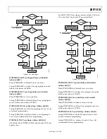
ADVANCE TOGGLE OF
FIELD BY PFTOG[4:0]
DELAY TOGGLE OF
FIELD BY PFTOG[4:0]
PFTOGSIGN
ODD FIELD?
0
1
NO
YES
PFTOGDELE
ADDITIONAL
DELAY BY
1 LINE
1
0
PFTOGDELO
ADDITIONAL
DELAY BY
1 LINE
1
0
FIELD
TOGGLE
NOT VALID FOR USER
PROGRAMMING
04984-029
Figure 29. PAL F Toggle
SYNC PROCESSING
The ADV7181B has two additional sync processing blocks that
postprocess the raw synchronization information extracted
from the digitized input video. If preferred, the blocks can be
disabled via the following two I
2
C bits.
ENHSPLL Enable Hsync Processor, Address 0x01[6]
The Hsync processor is designed to filter incoming Hsyncs that
have been corrupted by noise, providing improved performance
for video signals with stable time bases but poor SNR.
Setting ENHSPLL to 0 disables the Hsync processor.
Setting ENHSPLL to 1 (default) enables the Hsync processor.
ENVSPROC Enable Vsync Processor, Address 0x01[3]
This block provides extra filtering of the detected Vsyncs to give
improved vertical lock.
Setting ENVSPROC to 0
disables the Vsync processor.
Setting ENVSPROC to 1(default) enables the Vsync processor.
VBI DATA DECODE
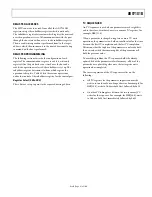
The following low data rate VBI signals can be decoded by the
ADV7181B:
•
Wide screen signaling (WSS)
•
Copy generation management systems (CGMS)
•
Closed captioning (CC)
•
EDTV
•
Gemstar 1×- and 2×-compatible data recovery
The presence of any of the above signals is detected and, if
applicable, a parity check is performed. The result of this testing
is contained in a confidence bit in the VBI Info[7:0] register.
Users are encouraged to first examine the VBI Info register
before reading the corresponding data registers. All VBI data
decode bits are read only.
All VBI data registers are double-buffered with the field signals.
This means that data is extracted from the video lines and
appears in the appropriate I
2
C registers with the next field
transition. They are then static until the next field.
The user should start an read sequence with VS by first
examining the VBI Info register. Then, depending on what data
was detected, the appropriate data registers should be read.
The data registers are filled with decoded VBI data even if their
corresponding detection bits are low; it is likely that bits within
the decoded data stream are wrong.

