ADV7181B
Rev. B | Page 9 of 100
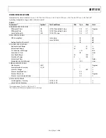
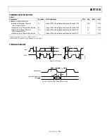
THERMAL SPECIFICATIONS
Table 5.
Parameter
1, 2
Symbol
Test
Conditions
Min
Typ
Max
Unit
THERMAL CHARACTERISTICS
Junction-to-Ambient Thermal
Resistance (Still Air)
θ
JA
4-layer PCB with solid ground plane, 64-lead LFCSP
45.5
°C/W
Junction-to-Case Thermal Resistance
θ
JC
4-layer PCB with solid ground plane, 64-lead LFCSP
9.2
°C/W
Junction-to-Ambient Thermal
Resistance (Still Air)
θ
JA
4-layer PCB with solid ground plane, 64-lead LQFP
47
°C/W
Junction-to-Case Thermal Resistance
θ
JC
4-layer PCB with solid ground plane, 64-lead LQFP
11.1
°C/W
1
Temperature range: T
MIN
to T
MAX
, –40°C to +85°C
2
The min/max specifications are guaranteed over this range.
TIMING DIAGRAMS
SDA
SCLK
t
3
t
5
t
3
t
4
t
8
t
6
t
7
t
2
t
1
04984-002
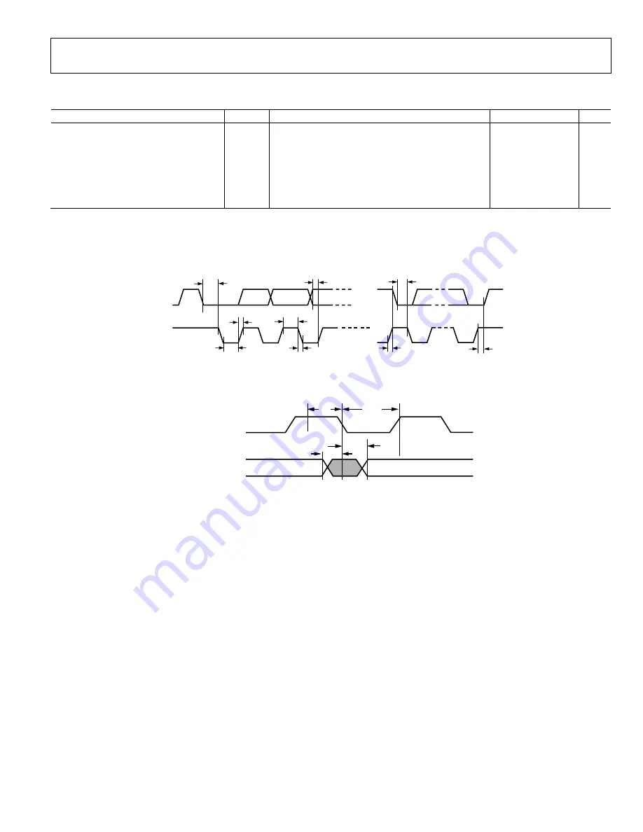
Figure 2. I
2
C Timing
OUTPUT LLC
OUTPUTS P0–P15, VS,
HS, FIELD,
SFL
t
9
t
10
t
11
t
12
04984-003
Figure 3. Pixel Port and Control Output Timing

