ADV8003 Hardware Manual
Rev. B, August 2013
361
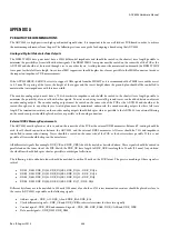
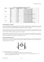
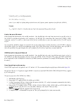
To find C1 and C2, use the following formula:
C1
=
C2
=
2(C
load
– C
stray
)
-
C
pg
where
C
stray
is usually 2 to 3 pF, depending on board traces and
C
pg
(pin-to-ground-capacitance) is 4 pF for the ADV8003.
Example:
C
load
= 30 pF,
C1
= 50 pF,
C2
= 50 pF (in this case, 47 pF is the nearest real-life cap value to 50 pF)
Encoder Component Placement
External component placement must be carefully considered – they should be kept as far away from noisy circuits as possible, as close to
the ADV8003 as possible and preferably on the same layer as the ADV8003. The external loop filter (connected to PVDD3), COMP,
termination resistors, V
REF
, and R
SETx
circuits must all be laid out carefully otherwise noise may couple onto the SD or HD encoder
outputs.
Any external filter and buffer components connected to the encoder analog outputs should be placed close to the ADV8003 to minimize
the possibility of noise cross talk between neighboring circuitry. The encoder analog output traces should be kept as short as possible to
reduce the possibility of any signal integrity issues and to minimize the effect of trace capacitance on output bandwidth.
HDMI Transmitter Component Placement
External component placement must be carefully considered – they should be kept as far away as possible from noisy circuits, as close to
the ADV8003 as possible and preferably on the same layer as the ADV8003. The R_TX1 and R_TX2 resistors and PVDD5 and PVDD6
power supplies must all be carefully laid out otherwise the HDMI transmitter performance, for example, HDMI compliance testing, may
be reduced.
Power Supply Design and Sequencing
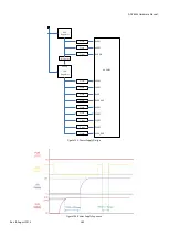
The ADV8003 requires only two regulators, one 3.3 V and one 1.8 V. The recommended power supply design is illustrated in
If using more than one 1.8 V regulator to supply ADV8003, it must be ensured that DVDD_DDR, PVDD_DDR and DVDD are supplied
by the same regulator.
The power-up sequence of the ADV8003 is as follows:
1.
Hold RESET and PDN pins low.
2.
Bring up the 3.3 V supplies (DVDD_IO, AVDD1, and AVDD2).
3.
A delay of a minimum of 20 ms is required from the point in which the 3.3 V reaches its minimum recommended value (that is,
3.14 V) before powering up the 1.8 V supplies.
4.
Bring up the 1.8 V supplies (DVDD, CVDD1, PVDD1, PVDD2, PVDD3, AVDD3, DVDD_DDR, and PVDD_DDR). These
should be powered up together, that is, there should be a difference of less than 0.3 V between them.
5.
RESET may be pulled high after supplies have been powered up.
6.
A complete RESET is recommended after power up. This can be performed by the system microcontroller.
Summary of Contents for ADV8003
Page 366: ...ADV8003 Hardware Manual Rev B August 2013 366 Figure 144 ADV8003 Schematic Page 4...
Page 367: ...ADV8003 Hardware Manual Rev B August 2013 367 Figure 145 ADV8003 Schematic Page 5...
Page 368: ...ADV8003 Hardware Manual Rev B August 2013 368 Figure 146 ADV8003 Schematic Page 6...
Page 369: ...ADV8003 Hardware Manual Rev B August 2013 369 Figure 147 ADV8003 Schematic Page 7...
Page 371: ...ADV8003 Hardware Manual Rev B August 2013 371 Figure 149 ADV8003 Schematic Page 9...
Page 372: ...ADV8003 Hardware Manual Rev B August 2013 372 Figure 150 ADV8003 Schematic Page 10...
Page 373: ...ADV8003 Hardware Manual Rev B August 2013 373 Figure 151 ADV8003 Schematic Page 11...
Page 374: ...ADV8003 Hardware Manual Rev B August 2013 374 Figure 152 ADV8003 Schematic Page 12...
Page 375: ...ADV8003 Hardware Manual Rev B August 2013 375 Figure 153 ADV8003 Schematic Page 13...
Page 376: ...ADV8003 Hardware Manual Rev B August 2013 376 Figure 154 ADV8003 Schematic Page 14...
Page 377: ...ADV8003 Hardware Manual Rev B August 2013 377 Figure 155 ADV8003 Schematic Page 15...
Page 378: ...ADV8003 Hardware Manual Rev B August 2013 378 Figure 156 ADV8003 Schematic Page 16...
Page 379: ...ADV8003 Hardware Manual Rev B August 2013 379 Figure 157 ADV8003 Schematic Page 17...
Page 380: ...ADV8003 Hardware Manual Rev B August 2013 380 Figure 158 ADV8003 Schematic Page 18...
Page 381: ...ADV8003 Hardware Manual Rev B August 2013 381 Figure 159 ADV8003 Schematic Page 19...
Page 382: ...ADV8003 Hardware Manual Rev B August 2013 382 Figure 160 ADV8003 Schematic Page 20...
Page 383: ...ADV8003 Hardware Manual Rev B August 2013 383 Figure 161 ADV8003 Schematic Page 21...
Page 384: ...ADV8003 Hardware Manual Rev B August 2013 384 Figure 162 ADV8003 Schematic Page 22...
Page 385: ...ADV8003 Hardware Manual Rev B August 2013 385 Figure 163 ADV8003 Schematic Page 23...
Page 386: ...ADV8003 Hardware Manual Rev B August 2013 386 Figure 164 ADV8003 Schematic Page 24...
Page 387: ...ADV8003 Hardware Manual Rev B August 2013 387 Figure 165 ADV8003 Schematic Page 25...
Page 388: ...ADV8003 Hardware Manual Rev B August 2013 388 Figure 166 ADV8003 Schematic Page 26...
Page 389: ...ADV8003 Hardware Manual Rev B August 2013 389 Figure 167 ADV8003 Schematic Page 27...
Page 390: ...ADV8003 Hardware Manual Rev B August 2013 390 Figure 168 ADV8003 Schematic Page 28...
Page 391: ...ADV8003 Hardware Manual Rev B August 2013 391 Figure 169 ADV8003 Schematic Page 29...
Page 392: ...ADV8003 Hardware Manual Rev B August 2013 392 Figure 170 ADV8003 Schematic Page 30...
Page 393: ...ADV8003 Hardware Manual Rev B August 2013 393 Figure 171 ADV8003 Schematic Page 31...
Page 395: ...ADV8003 Hardware Manual Rev B August 2013 395 Figure 173 ADV8003 Layout Page 2...
Page 396: ...ADV8003 Hardware Manual Rev B August 2013 396 Figure 174 ADV8003 Layout Page 3...
Page 397: ...ADV8003 Hardware Manual Rev B August 2013 397 Figure 175 ADV8003 Layout Page 4...
Page 398: ...ADV8003 Hardware Manual Rev B August 2013 398 Figure 176 ADV8003 Layout Page 5...
Page 399: ...ADV8003 Hardware Manual Rev B August 2013 399 Figure 177 ADV8003 Layout Page 6...
Page 400: ...ADV8003 Hardware Manual Rev B August 2013 400 Figure 178 ADV8003 Layout Page 7...
Page 401: ...ADV8003 Hardware Manual Rev B August 2013 401 Figure 179 ADV8003 Layout Page 8...
Page 427: ...ADV8003 Hardware Manual Rev B August 2013 427 P 2 Z Z Z P 1 Z Z Z P 0 Z Z Z...

