background image


ADV8003 Hardware Manual 


Rev. B, August 2013 

     182 


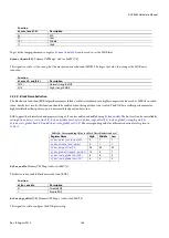
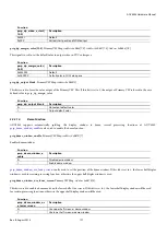
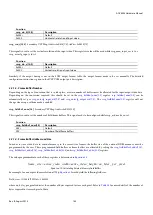
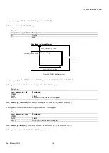
svsp_enable_vom

, Secondary VSP Map, 

Address 0xE610[5] 

 
This bit is used to control the Video Output Module (VOM). If this bit is set to 1, the VOM is enabled to read video data from external 
memory, process it and then output it. 
 

Function 


svsp_enable_vom 

Description 

0  

Disable VOM 

Enable VOM 

 
If using the SVSP, the FFS must be enabled (using 

svsp_enable_ffs

) so that the hardware knows the various conversions that must be 

performed. The use of field/frame buffers in external memory is managed by the FFS which decides which frame buffer should be used by 

the VIM to store input video data. The FFS also decides which frame buffer should be read back by the VOM. The SVSP utilizes a frame 
repeat/drop mechanism to implement FRC, which is also managed by the FFS. 
 

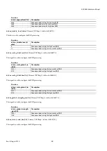
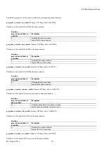
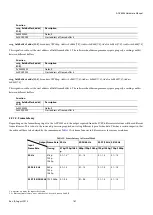
svsp_enable_ffs

, Secondary VSP Map, 

Address 0xE610[7] 

 
This bit is used to control the Field Frame Scheduler (FFS). If this bit is set to 1, the FFS is enabled and the VIM and VOM are 
scheduled by the FFS, which means the Secondary VSP is in work mode. If this bit is set to 0, the Secondary VSP is in idle mode. 
 

Function 


svsp_enable_ffs 

Description 

0  

Disable FFS/FRC 

Enable FFS/FRC 


3.3.1.1.


Autoconfiguration 

Each block inside the  VIM and the  VOM can be automatically configured to decrease the configuration complexity. The 

svsp_autocfg_input_vid[7:0]


and 

svsp_autocfg_output_vid[7:0]

  registers  should be set to make the autoconfiguration work. The 

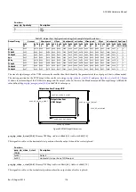
59.94/23.97 Hz timings have the same VID as the corresponding 60/24 Hz timing in 

Table 31


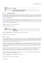
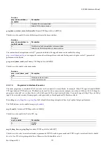
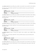
svsp_autocfg_input_vid[7:0]

, Secondary VSP Map, 

Address 0xE660[7:0] 

 
This register is used to set the input timing VIC. If this register is 0, SVSP will use values in registers of svsp_vin_h, svsp_vin_v and 

svsp_vin_fr to set input video. 
 

Function 


svsp_autocfg_input_vid
[7:0] 

Description 

0x00  

Custom input video 

0xXX 

Input timing VIC 


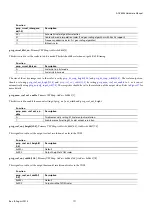
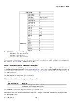
Table 31: SVSP Supported Input Video Timing and VID 

Video Timing 

VID 

CEA 
 

640x480p60 

720x480p60 

2 or 3 or 14 or 15 or 35 or 36 

720x240p60 

8 or 9 or 12 or 13 

1280x720p60 

1920x1080p 

16 

720x576p50 

17 or 18 or 29 or 30 or 37 or 38 

1280x720p50 

19 

720x288p50 

23 or 24 or 27 or 28 

1920x1080p50 

31 

Summary of Contents for ADV8003

Page 1: ...ADV8003 Video Signal Processor with Motion Adaptive De interlacing Scaling Bitmap OSD Dual HDMI Tx and Video Encoder HARDWARE MANUAL Rev B August 2013...

Page 2: ...r 19 1 1 7 Video Encoder 19 1 2 Main Features of the ADV8003 19 1 2 1 Video Signal Processor 19 1 2 1 1 Primary VSP 19 1 2 1 2 Secondary VSP 20 1 2 2 OSD 20 1 2 3 Video Encoder 20 1 2 4 HDMI 1 4 Trans...

Page 3: ...5 4 DDR2 Loopback Test 117 2 2 6 I2 C Auto Increment 118 2 2 7 SPI Loop Through 119 2 2 8 VBI Data Insertion 119 2 2 8 1 Extraction Overview 119 2 2 8 2 Ancillary Data Extraction 120 2 2 8 3 SPI Data...

Page 4: ...de 172 3 2 3 13 Output Port 173 3 2 3 14 Demo Function 177 3 2 3 15 Progressive to Interlaced Converter 179 3 2 3 16 Automatic Contrast Enhancement 180 3 3 Secondary VSP 180 3 3 1 Introduction to SVSP...

Page 5: ...erview 218 4 2 8 2 SPI Slave Interface 223 4 2 8 3 SPI Master Interface 225 4 2 9 OSD Initialization 226 5 Serial Video Receiver 227 5 1 5 V Detect 227 5 2 TMDS Clock Activity Detection 228 5 3 Clock...

Page 6: ...cture 260 6 11 2 Audio Configuration 261 6 11 2 1 I2S Audio 263 6 11 2 2 SPDIF Audio 270 6 11 2 3 DSD Audio 271 6 11 2 4 HBR Audio 271 6 11 3 N and CTS Parameters 272 6 11 3 1 N Parameter 273 6 11 3 2...

Page 7: ...Control 314 8 4 5 1 Programming the FSC 315 8 4 6 SD Noninterlaced Mode 240p 288p 315 8 4 7 Filters 315 8 4 7 1 SD Filters 315 8 4 7 2 ED HD Filters 318 8 4 8 ED HD Test Pattern Generator 319 8 4 9 C...

Page 8: ...duction 350 9 2 2 Interrupt Architecture Overview 354 9 2 2 1 Multiple Interrupt Events 355 9 2 3 Serial Video Interrupts Validity Checking Process 355 9 3 VSP and OSD Section 355 9 3 1 Interrupt Arch...

Page 9: ...ADV8003 Hardware Manual Rev B August 2013 9 Appendix F 416 Pixel Input and Output Formats 416 List of Figures 431 List of Tables 435 List of Equations 437 Revision History 438...

Page 10: ...mber is referred to as Bit 0 V X Y Bit field representation covering bit X to Y of a value or a field V 0xNN Hexadecimal base 16 numbers are preceded by the prefix 0x 0bNN Binary base 2 numbers are pr...

Page 11: ...T Device Under Test designate the ADV8003 unless stated otherwise DVD Digital Video Disc DVI Digital Visual Interface EAV End of Active Video ED Enhanced Definition ENC Encoder EQ Equalizer FFS Field...

Page 12: ...te SMPTE Society of Motion Picture and Television Engineers SNR Signal to Noise Ratio SOG Sync on Green SOY Sync on Y SPA Source Physical Address SPD Source Production Product Descriptor SPDIF Sony Ph...

Page 13: ...dress 0xE20B 7 6 Read Only A readback of the deep color mode information extracted from the general control packet Function deep_color_mode 1 0 Description 00 8 bits per channel 01 10 bits per channel...

Page 14: ...endation ITU R BT 601 February 1998 ITU ITU R BT 601 5 Studio encoding parameters of digital television for standard 4 3 and widescreen 16 9 aspect ratios December 1995 ITU ITU R BT 709 5 Parameter va...

Page 15: ...outputs for example 1080p60 on HDMI TX1 and 720p on HDMI TX2 and the HD encoder The primary VSP PVSP in the ADV8003 is capable of upscaling from 480i to 4k x 2k formats The secondary VSP SVSP in the A...

Page 16: ...relevant to a particular generic this is indicated in the introduction to that section 1 1 1 Digital Video Input Video data can be input into the ADV8003 in a number of ways The flexible 60 bit TTL in...

Page 17: ...e details 1 1 3 Video Signal Processor The motion adaptive de interlacer in the ADV8003 offers excellent edge detection and ultra low angle performance The per pixel de interlacing algorithm used deli...

Page 18: ...ures buttons and so on Individual regions can be alpha blended and prioritized versus other regions OSD Build OSD Scaler OSD Blend Video External OSD DDR2 OSD Build OSD Scaler OSD Blend Video 1 Extern...

Page 19: ...he single transmitter variants of the ADV8003 are ADV8003KBCZ 8B 7B The ADV8003KBCZ 7T does not feature any HDMI transmitters 1 1 7 Video Encoder The ADV8003 features a high speed digital to analog vi...

Page 20: ...g external memory bandwidth Blending onto 3 GHz video formats for ADV8003KBCZ 8x derivatives Pixel by pixel alpha blending of OSD data on video data Option of externally generated OSD OSD can be overl...

Page 21: ...DCP KEYS CEC CONTROL HDCP AND EDID UNCONTROLLER AUDIO DATA CAPTURE I2C MASTER TMDS OUTPUTS HDCP ENCRYPTION HDCP KEYS TMDS OUTPUTS REFERENCE AND CABLE DETECTION 4 2 2 4 4 4 AND COLOR SPACE CONVERTER HD...

Page 22: ...GND DDC2_ SDA P 19 P 18 P 17 P 16 TX2_0 TX2_0 GND HPD_ TX2 GND GND P 15 P 14 TX2_C TX2_C GND R_TX2 HEAC_ 2 HEAC_ 2 PVDD6 GND AVDD3 PVDD6 TEST3 GND DDR_ DQ 6 GND DVDD DVDD DVDD DDR_ DQ 9 DDR_ DQ 14 GND...

Page 23: ...omplement Input A20 RX_2N Rx input Rx Channel 2 Complement Input A21 CVDD1 Power Comparator Supply Voltage 1 8 V A22 RSET1 Miscellaneous analog1 Resistor Current Setting for Encoder DACs DAC1 DAC2 and...

Page 24: ...a 3 3V supply C8 SCK1 Serial port control Serial Clock Serial Port 1 Serial Port 1 is used for OSD control C9 GND GND Ground C10 INT0 Miscellaneous digital Interrupt Pin 0 When status bits change thi...

Page 25: ...ation resistance Use a 500 resistor between this pin and GND Place the RTERM resistor as close as possible to the ADV8003 D20 AVDD2 Power Analog Power Supply 3 3 V D21 AVDD2 Power Analog Power Supply...

Page 26: ...D Ground G20 ELPF1 Miscellaneous analog1 External Loop Filter for PLL 1 Connected to PVDD3 G21 ELPF2 Miscellaneous analog1 External Loop Filter for PLL 2 Connected to PVDD3 G22 GND GND Ground G23 AVDD...

Page 27: ...or Digital Input Video K3 DVDD_IO Power Digital Interface Supply 3 3 V K4 DVDD_IO Power Digital Interface Supply 3 3 V K7 GND GND Ground K8 GND GND Ground K9 GND GND Ground K10 GND GND Ground K11 GND...

Page 28: ...a 470 resistor 1 tolerance between this pin and ground The external resistor should be placed as close as possible to the ADV8003 M21 PVDD5 Power1 HDMI Tx PLL Power Supply 1 8 V This pin is a voltage...

Page 29: ...D GND Ground P22 TX2_2 HDMI Tx2 HDMI2 Channel 2 True Output P23 TX2_2 HDMI Tx2 HDMI2 Channel 2 Complementary Output R1 P 16 Digital video input Digital Video Input Bus 35 0 R2 P 17 Digital video input...

Page 30: ...D GND Ground U20 R_TX2 HDMI Tx21 Sets internal reference currents Place a 470 resistor 1 tolerance between this pin and ground The external resistor should be placed as close as possible to the ADV800...

Page 31: ...Power DDR Interface Supply 1 8 V Y19 DDR_DQ 14 DDR interface Data Line Interface to external RAM data lines Y20 GND GND Ground Y21 DDR_DQ 6 DDR interface Data Line Interface to external RAM data line...

Page 32: ...interface Data Line Interface to external RAM data lines AB21 DDR_DQ 5 DDR interface Data Line Interface to external RAM data lines AB22 DDR_DQS 0 DDR interface Data Strobe for DDR Data Bytes 7 0 AB2...

Page 33: ...scription AC22 DDR_DQS 0 DDR interface Data Strobe for DDR Data Byte 7 0 AC23 DDR_DQ 1 DDR interface Data Line Interface to external RAM data lines 1 Sensitive node Careful layout is important The ass...

Page 34: ...P 21 P 20 GND P 19 P 18 P 17 P 16 GND GND GND P 15 P 14 GND PVDD6 GND AVDD3 PVDD6 TEST3 GND DDR_ DQ 6 GND DVDD DVDD DVDD DDR_ DQ 9 DDR_ DQ 14 GND GND DDR_ A 4 DDR_ A 11 GND DDR_ DQS 3 DDR_ DQ 23 PVDD_...

Page 35: ...CN Rx input Rx Clock Complement Input A18 RX_0N Rx input Rx Channel 0 Complement Input A19 RX_1N Rx input Rx Channel 1 Complement Input A20 RX_2N Rx input Rx Channel 2 Complement Input A21 CVDD1 Power...

Page 36: ...round C10 INT0 Miscellaneous digital Interrupt Pin 0 When status bits change this pin is triggered C11 PDN Miscellaneous digital Power Down This pin controls the power state of the ADV8003 C12 GND GND...

Page 37: ...this pin D23 NC No connect Do not connect to this pin E1 OSD_IN 13 VBI_SCK OSD video input miscellaneous digital External OSDVideo Pixel Input Port OSD_IN 13 Serial Clock forVBI Data Serial Port VBI_...

Page 38: ...deo Pixel Input Port OSD_IN 2 H3 OSD_IN 3 OSD video input External OSD Video Pixel Input Port OSD_IN 3 H4 OSD_IN 4 OSD video input External OSD Video Pixel Input Port OSD_IN 4 H7 GND GND Ground H8 GND...

Page 39: ...D Ground K14 GND GND Ground K15 GND GND Ground K16 GND GND Ground K17 GND GND Ground K20 DDC1_SCL HDMI Tx1 HDCP Slave Serial Clock for HDMI Tx1 This pin is open drain use a 2 k resistor to connect thi...

Page 40: ...C from HDMI Connector M23 HEAC_1 HDMI Tx1 HDMI Tx1 HEC from HDMI Connector N1 P 24 Digital video input Digital Video Input Bus 35 0 N2 P 25 Digital video input Digital Video Input Bus 35 0 N3 P 26 Dig...

Page 41: ...ital video input Digital Video Input Bus 35 0 R7 GND GND Ground R8 GND GND Ground R9 GND GND Ground R10 GND GND Ground R11 GND GND Ground R12 GND GND Ground R13 GND GND Ground R14 GND GND Ground R15 G...

Page 42: ...video input Digital Video Input Bus 35 0 V20 GND GND Ground V21 PVDD6 Power1 HDMI Tx PLL Power Supply 1 8 V This pin is a voltage regulator output Connect a decoupling capacitor between this pin and g...

Page 43: ...ns do not connect to this pin For designs that must maintain consistency with the ADV8002 this pin can be grounded AA9 DDR_A 8 DDR interface Address Line Interface to external RAM address lines AA10 D...

Page 44: ...C4 DDR_DQ 25 DDR interface Data Line Interface to external RAM data lines AC5 DDR_DQ 28 DDR interface Data Line Interface to external RAM data lines AC6 DDR_DQ 27 DDR interface Data Line Interface to...

Page 45: ...TEST3 GND DDR_ DQ 6 GND DVDD DVDD DVDD DDR_ DQ 9 DDR_ DQ 14 GND GND DDR_ A 4 DDR_ A 11 GND DDR_ DQS 3 DDR_ DQ 23 PVDD_ DDR DVDD_ DDR DDR_ CK DVDD_ DDR DDR_ CAS DVDD_ DDR DVDD_ DDR P 13 P 12 P 11 P 10...

Page 46: ...ock Complement Input A18 RX_0N Rx input Rx Channel 0 Complement Input A19 RX_1N Rx input Rx Channel 1 Complement Input A20 RX_2N Rx input Rx Channel 2 Complement Input A21 CVDD1 Power Comparator Suppl...

Page 47: ...d C10 INT0 Miscellaneous digital Interrupt Pin 0 When status bits change this pin is triggered C11 PDN Miscellaneous digital Power Down This pin controls the power state of the ADV8003 C12 GND GND Gro...

Page 48: ...pin D23 NC No connect Do not connect to this pin E1 OSD_IN 13 VBI_SCK OSD video input miscellaneous digital External OSD Video Pixel Input Port OSD_IN 13 Serial Clock for VBI Data Serial Port VBI_SCK...

Page 49: ...deo Pixel Input Port OSD_IN 2 H3 OSD_IN 3 OSD video input External OSD Video Pixel Input Port OSD_IN 3 H4 OSD_IN 4 OSD video input External OSD Video Pixel Input Port OSD_IN 4 H7 GND GND Ground H8 GND...

Page 50: ...D Ground K14 GND GND Ground K15 GND GND Ground K16 GND GND Ground K17 GND GND Ground K20 DDC1_SCL HDMI Tx1 HDCP Slave Serial Clock for HDMI Tx1 This pin is open drain use a 2 k resistor to connect thi...

Page 51: ...DMI Connector M23 HEAC_1 HDMI Tx1 HDMI Tx1 HEC from HDMI Connector N1 P 24 Digital video input Digital Video Input Bus 35 0 N2 P 25 Digital video input Digital Video Input Bus 35 0 N3 P 26 Digital vid...

Page 52: ...Video Input Bus 35 0 R4 P 19 Digital video input Digital Video Input Bus 35 0 R7 GND GND Ground R8 GND GND Ground R9 GND GND Ground R10 GND GND Ground R11 GND GND Ground R12 GND GND Ground R13 GND GN...

Page 53: ...Complementary Output V1 P 6 Digital video input Digital Video Input Bus 35 0 V2 P 7 Digital video input Digital Video Input Bus 35 0 V3 P 8 Digital video input Digital Video Input Bus 35 0 V4 P 9 Dig...

Page 54: ...Interface to external RAM data lines AA6 DVDD_DDR Power DDR Interface Supply 1 8 V AA7 DDR_DQS 3 DDR interface Data Strobe for DDR Data Byte 31 24 AA8 NC GND No connect GND For new ADV8003 designs do...

Page 55: ...to external RAM data lines AC3 DDR_DQ 22 DDR interface Data Line Interface to external RAM data lines AC4 DDR_DQ 25 DDR interface Data Line Interface to external RAM data lines AC5 DDR_DQ 28 DDR inte...

Page 56: ...ND GND P 15 P 14 GND PVDD6 GND AVDD3 PVDD6 TEST3 GND DDR_ DQ 6 GND DVDD DVDD DVDD DDR_ DQ 9 DDR_ DQ 14 GND GND DDR_ A 4 DDR_ A 11 GND DDR_ DQS 3 DDR_ DQ 23 PVDD_ DDR DVDD_ DDR DDR_ CK DVDD_ DDR DDR_ C...

Page 57: ...x input Rx Channel 1 Complement Input A20 RX_2N Rx input Rx Channel 2 Complement Input A21 CVDD1 Power Comparator Supply Voltage 1 8 V A22 NC No connect Do not connect to this pin A23 NC No connect Do...

Page 58: ...DD1 Power HDMI Rx Inputs Analog Supply 3 3 V C18 GND GND Ground C19 GND GND Ground C20 AVDD1 Power HDMI Rx Inputs Analog Supply 3 3 V C21 AVDD1 Power HDMI Rx Inputs Analog Supply 3 3 V C22 NC No conne...

Page 59: ...o Pixel Input Port OSD_IN 9 F2 OSD_IN 10 OSD video input External OSD Video Pixel Input Port OSD_IN 10 F3 OSD_IN 11 OSD video input External OSD Video Pixel Input Port OSD_IN 11 F4 OSD_IN 12 OSD video...

Page 60: ...External OSD Video Pixel Input Port OSD_IN 0 J7 DVDD Power Digital Power Supply 1 8 V J8 GND GND Ground J9 GND GND Ground J10 GND GND Ground J11 GND GND Ground J12 GND GND Ground J13 GND GND Ground J...

Page 61: ...o this pin M1 P 28 Digital video input Digital Video Input Bus 35 0 M2 P 29 Digital video input Digital Video Input Bus 35 0 M3 P 30 Digital video input Digital Video Input Bus 35 0 M4 P 31 Digital vi...

Page 62: ...wer Supply 1 8 V P8 GND GND Ground P9 GND GND Ground P10 GND GND Ground P11 GND GND Ground P12 GND GND Ground P13 GND GND Ground P14 GND GND Ground P15 GND GND Ground P16 GND GND Ground P17 DVDD Power...

Page 63: ...us 35 0 U7 GND GND Ground U8 GND GND Ground U9 DVDD Power Digital Power Supply 1 8 V U10 GND GND Ground U11 GND GND Ground U12 DVDD Power Digital Power Supply 1 8 V U13 GND GND Ground U14 GND GND Grou...

Page 64: ..._DQ 9 DDR Interface Data Line Interface to external RAM data lines Y18 DVDD_DDR Power DDR Interface Supply 1 8 V Y19 DDR_DQ 14 DDR interface Data Line Interface to external RAM data lines Y20 GND GND...

Page 65: ...Data Line Interface to external RAM data lines AB22 DDR_DQS 0 DDR interface Data Strobe for DDR Data Bytes 7 0 AB23 DDR_DQ 4 DDR interface Data Line Interface to external RAM data lines AC1 DDR_DQ 16...

Page 66: ...ADV8003 Hardware Manual Rev B August 2013 66 1 Sensitive node Careful layout is important The associated circuitry should be kept as close as possible to the ADV8003...

Page 67: ...for this subaddress register This means that I2 C writes to the part will be in the form I2 C Address Address MSBs Address LSBs Data For example to write 0xFF to the encoder register map register 0x5...

Page 68: ...ister Address LSBs Data ACK R W 1 8 1 8 ACK ACK ACK SDA SCL S 1 7 8 9 9 9 P Device Address 1 8 9 Register Address MSBs Register Address LSBs Data ACK R W 1 8 1 8 ACK ACK ACK S 1 7 8 9 9 9 P Device Add...

Page 69: ...rforms motion adaptive de interlacing as well as scaling ACE FRC cadence detection CUE correction RNR BNR and MNR PVSP utilizes the external DDR2 memory for such processes as FRC de interlacing and RN...

Page 70: ...Yes 3 No Mode 3 2 No if using SVSP 1 No Mode 4 2 Yes 2 No Mode 5 3 No if using SVSP 3 No Mode 6 2 No if using SVSP 1 No Mode 7 1 2 Yes 1 2 Yes Mode 8 1 2 Yes 1 2 Yes Mode 9 Bypass 1 Yes 0 Yes Mode 10...

Page 71: ...core must then be selected This can be placed before the PVSP and both the input video and OSD can be scaled at the same time However depending on the application the optimal solution may be to have b...

Page 72: ...1080i 1080p 720p 480i 480i Primary VSP HDMI Tx2 HDMI Tx1 HD Encoder SD Encoder 480i Video from Decoder Video 36 bit Input Port Exosd 24 bit Input Port Serial Video RX Input Muxing Secondary Data Forma...

Page 73: ...erlaced 1080i 1080p 720p 480i 480i Primary VSP HDMI Tx2 HDMI Tx1 HD Encoder SD Encoder Video 36 bit Input Port Exosd 24 bit Input Port Serial Video RX 480i Video from Decoder 480i Input Muxing Seconda...

Page 74: ...HDMI Tx1 HD Encoder SD Encoder 480p Video from Transceiver Video 36 bit Input Port Exosd 24 bit Input Port Serial Video RX Input Muxing Secondary Data Formatting CSC Primary Data Formatting CSC ACE R...

Page 75: ...I Tx2 HDMI Tx1 HD Encoder SD Encoder 480p Video from Transceiver Video 36 bit Input Port Exosd 24 bit Input Port Serial Video RX Input Muxing Secondary Data Formatting CSC Primary Data Formatting CSC...

Page 76: ...der 480p Video 36 bit Input Port Exosd 24 bit Input Port Serial Video RX Input Muxing Secondary Data Formatting CSC Primary Data Formatting CSC ACE RX Data Formatting CSC Video Muxing Figure 19 ADV800...

Page 77: ...Tx2 HDMI Tx1 HD Encoder SD Encoder 480p Video from Decoder 720p Video 36 bit Input Port Exosd 24 bit Input Port Serial Video RX Input Muxing Secondary Data Formatting CSC Primary Data Formatting CSC...

Page 78: ...der SD Encoder 720p Video from Transceiver 720p Video 36 bit Input Port Exosd 24 bit Input Port Serial Video Rx Input Muxing Secondary Data Formatting CSC Primary Data Formatting CSC ACE RX Data Forma...

Page 79: ...ry VSP 720p Video from Transceiver 720p Video 36 bit Input Port Exosd 24 bit Input Port Serial Video RX Input Muxing Secondary Data Formatting CSC Primary Data Formatting CSC ACE RX Data Formatting CS...

Page 80: ...ing CSC Primary Data Formatting CSC ACE RX Data Formatting CSC Video Muxing OSD Blend Build OSD Scale OSD Secondary VSP Output Muxing HDMI Tx2 HDMI Tx1 HD Encoder SD Encoder Mode 9 Bypass DDR2 Memory...

Page 81: ...Scale OSD Secondary VSP Output Muxing Mode 10 PiP External OSD 720p DDR2 Memory Interface OSD rendered at a single set resolution 480p 480p 1080p 1080p 1080p PiP 480p OSD only 1080p PiP 480p OSD Data...

Page 82: ...data as one OSD region and blends this region with input video from Decoder OSD Blend Build OSD Scale OSD Secondary VSP Output Muxing Mode 11 PiP External OSD 720p DDR2 Memory Interface OSD rendered...

Page 83: ...ut Muxing Mode 12 PiP External OSD 720p DDR2 Memory Interface OSD rendered at a single set resolution 480p 480p Configurable 1080p 1080p 720p 1080p Primary VSP HDMI Tx2 HDMI Tx1 HD Encoder SD Encoder...

Page 84: ...Muxing 1080p Video from Decoder OSD Blend Build OSD Scale OSD Secondary VSP Output Muxing Mode 13 DDR2 Memory Interface 720p 1080p 1080p 1080p OSD 480p OSD only 1080p OSD 480p OSD Data Only 1080p HDM...

Page 85: ...imary Data Formatting CSC ACE RX Data Formatting CSC Video Muxing Figure 28 ADV8003 Mode 14 Configuration Mode 14 is used to support three independent video streams The independent video streams are i...

Page 86: ...nnel Secondary Input Channel 2_ RX Input Channel RX Input Channel OSD Blend 2 Primary VSP PtoI OSD Blend 1 Secondary VSP Secondary Input Channel Primary Input Channel RX Input Channel OSD Blend 2 Prim...

Page 87: ...0x03 From Internal OSD Blend 1 0x04 From Secondary VSP PtoI Converter 0x05 From OSD TTL Input 0x06 From RX Input 0x07 From Internal OSD Blend 2 hd_enc_inp_sel 3 0 IO Map Address 0x1A04 7 4 This signal...

Page 88: ...om Internal OSD OSD only no blend 0x04 From Secondary Input Channel 0x05 From RX Input pvsp_inp_sel 3 0 IO Map Address 0x1A05 3 0 This signal is used to select the video source for the Primary VSP Fun...

Page 89: ...tput from Primary VSP to OSD blend These four register writes configure the hardware blocks in the ADV8003 in mode 3 More registers will need to be configured depending on the input and desired video...

Page 90: ...igure 32 RX Input Channel 2 2 2 1 Video TTL Input The video TTL input pins are defined as follows P 47 0 HS VS DE PCLK The video TTL input pins can be connected to either the primary input channel ref...

Page 91: ...TTL clock are output on the following pins OSD_IN 23 0 P 35 24 OSD_HS OSD_VS OSD_DE OSD_CLK The video data can be output at pixel frequencies up to 162 MHz Only single data rate video is supported on...

Page 92: ...iption 0 Disable TTL output 1 Enable TTL output ttl_out_sel 2 0 IO Map Address 0x1A02 2 0 This signal is used to select the video source for the TTL video output Function ttl_out_sel 2 0 Description 0...

Page 93: ...ut pins the EXOSD TTL input pins or the high speed TTL input pins using p_inp_chan_sel 1 0 If the primary input channel is connected to the video TTL input pins the format and bit width of the data fo...

Page 94: ...ts wide and is divided into three data channels Top D 35 24 Middle D 23 12 and Bottom D 11 0 This register allows the user to swap the order of these three data channels Function vid_swap_bus_ctrl 2 0...

Page 95: ...a sequence of Cr Cb Cr Cb vid_swap_cb_cr_422 IO Map Address 0x1B49 7 This bit is used to swap the order of the C data when decoding 4 2 2 data Function vid_swap_cb_cr_422 Description 0 Cb Cr decoding...

Page 96: ...D polarity does not change 1 Input FLD polarity gets inverted vid_hs_vs_mode is used to select the method by which the input video will be synchronized This may be required when the ADV8003 is used in...

Page 97: ...are replicated or not Codes replicated 4 4 4 FF FF FF 00 00 00 00 00 00 AV AV AV Codes not replicated FF 00 00 AV Function vid_av_codes_rep_man Description 1 AV codes are replicated 0 AV codes are not...

Page 98: ...e has a range of 1024 to 1016 Refer to Figure 36 for more information on how the brightness controls influence the video signal The saturation 7 0 value has a range 0 to 1 992 Refer to Figure 37 for m...

Page 99: ...ster uses 1 7 notation Function saturation 7 0 Description 0x00 Gain of 0 0x80 Unity Gain 0xFF Gain of 2 blank_level_u 11 0 IO Map Address 0x1A26 7 0 Address 0x1A27 7 4 This signal is used to adjust t...

Page 100: ...o TTL input pins or the EXOSD TTL input pins using s_inp_chan_sel 1 0 If the secondary input channel is connected to the video TTL input pins the format and bit width of the data for example 2 x 8 bit...

Page 101: ...7 0 011 D 15 8 D 23 16 D 7 0 100 D 7 0 D 23 16 D 15 8 101 D 7 0 D 15 8 D 23 16 110 D 15 8 D 7 0 D 23 16 111 D 23 16 D 15 8 D 7 0 The input formatter also has a number of controls which can be used to...

Page 102: ...rder of the C data when decoding 4 2 2 data Function exosd_swap_cb_cr_422 Description 0 Cb Cr decoding 1 Cr Cb decoding exosd_ps444_r444_conv is used to convert from pseudo 444 video data to real 444...

Page 103: ...xternal OSD DE timing signal Function exosd_de_pol Description 0 Input DE polarity doesn t change 1 Input DE polarity gets inverted exosd_hs_vs_mode is used to select the method by which the input vid...

Page 104: ...ot Codes replicated 4 4 4 FF FF FF 00 00 00 00 00 00 AV AV AV Codes not replicated FF 00 00 AV Function exosd_av_codes_rep_m an Description 1 AV codes are replicated 0 AV codes are not replicated The...

Page 105: ...s disabled which means that the updither block cannot be bypassed The updither block configuration is outlined in Section 2 2 3 The updither settings are shared for all channels primary secondary and...

Page 106: ...4 to 12 bit down dithering 12 to 10 bit down dithering Figure 39 Updither Operation updither_level 1 0 is used to configure the updither algorithm level This should be configured depending on the inpu...

Page 107: ...y rx_in_id Y Cb Cr HS VS CK P 35 P 0 VS HS DE Rx2 Rx2 Rx1 Rx1 Rx0 Rx0 RxC RxC Y Cb Cr HS VS CK Y Cb Cr HS VS CK P 35 P 0 VS HS DE Y Cb Cr HS VS CK OSD_IN 35 OSD_IN 0 OSD_VS OSD_HS OSD_DE Y Cb Cr HS VS...

Page 108: ...20x1080p 60Hz 0x12 720x576p 50Hz 0x13 1280x720p 50Hz 0x14 1920x1080i 50Hz 0x16 720 1440 x576i 50Hz 0x18 720 1440 x288p 50Hz 0x1A 2880 x576i 50Hz 0x1C 2880 x288p 50Hz 0x1E 1440x576p 50Hz 0x1F 1920x1080...

Page 109: ...17 CEA 861 VIC 23 288p_50 0x18 CEA 861 VIC 24 288p_50 0x1F CEA 861 VIC 31 1080p_50 0xFC CEA 861 VIC 252 288p_50 0xFD CEA 861 VIC 253 240p_60 0xFE CEA 861 VIC 254 480i_60 0xFF CEA 861 VIC 255 576i_50 r...

Page 110: ...ting DPLL Clock Period where output_clock_period is the period of the desired output sampling frequency For example for HD video the output clock sampling frequency would be 148 5 MHz This equation re...

Page 111: ...given equations pvsp_vid_clk_update IO Map Address 0x1A3A 4 This bit is used to trigger the open loop period to be captured in the DPLL A low to high transition triggers the action Function pvsp_vid_c...

Page 112: ...be fully frequency and phase locked using pvsp_err_sel If phase locked is selected there will be an integer frame latency from input to output If frequency locked is selected there could be a non inte...

Page 113: ...his bit is used to enable tracking of the frequency error to reduce the number of dropped repeated frames for the Secondary VSP Function svsp_track_en Description 0 Do not adjust for frequency differe...

Page 114: ...o indicate the burst length of the read write transaction Function burst_length 2 0 Description 010 Burst of 4 011 Burst of 8 rw_ctrl_oe sets the direction for several of the pins on the DDR2 memory i...

Page 115: ...2 2 5 2 DDR2 Bandwidth and Memory Selection The DDR2 interface on ADV8003 can be configured to work with one or two default DDR2 memories Using a single DDR2 memory limits the amount of functionality...

Page 116: ...080P24 32 24bit Supported Supported Not Supported Not Supported 1080P60 1080P24 16bit Supported Supported Supported Supported Motion Adaptive De interlacing SD ED input Supported Supported Supported S...

Page 117: ...allow testing of the ADV8003 DDR2 interface When the loopback test block is enabled it controls the commands sent to the DDR2 controller of the ADV8003 and generates pseudo random data and addresses...

Page 118: ...est_done IO Map Address 0x1AE1 0 Read Only This bit is used to readback the DDR2 loopback test has completed Function lbk_test_done Description 0 Test not complete 1 Loopback test finished lbk_test_re...

Page 119: ...0 Regular SPI mode 1 SPI slave clock routed to SPI master clock output 2 2 8 VBI Data Insertion ADV8003 supports VBI data such as CGMS WSS and CCAP insertion into the video stream through either the...

Page 120: ...rammed in 1A 1A4A 7 0 and 1A 1A4B 7 0 The format of the ancillary data packet is shown in Table 13 Table 13 Output Mode Outline Byte B9 B8 B7 B6 B5 B4 B3 B2 B1 B0 Description 0 0 0 0 0 0 0 0 0 0 0 Anc...

Page 121: ...either the rising or falling edge of the input VSync The output VBI data is muxed directly with the VBI data from the encoder register map before being output by the encoder vbi_src IO Map Address 0x1...

Page 122: ...ary stream with VBI decoded data 2 2 9 Resets This section documents the register bits used for resetting various sections of the ADV8003 These resets can be used by the system controller to reset ind...

Page 123: ...set IO Map Address 0x1AFD 2 Self Clearing This register bit resets the clock for the digital core Function sys_clk_reset Description 0 Default 1 Reset osd_reset IO Map Address 0x1AFD 1 Self Clearing T...

Page 124: ...ing This bit is used to reset the HDMI TX1 Function tx1_reset Description 0 Default 1 Reset dpll_reset IO Map Address 0x1AFE 2 Self Clearing This bit is used to reset the DPLL clock generator Function...

Page 125: ...n Mosquito Noise Reduction Block Noise Reduction Detail Enhancement Scaling and Frame Rate Conversion YUV Scaler 1 Scaler 2 Frame Rate Converter OSD Generation RGB Bitmap OSD Controller OSD Scaler C S...

Page 126: ...lues selected Function de_v_beg_e_pos 6 0 Description 0xXX Assert de when lcount reaches 0xXX on even fields de_v_beg_o_pos 6 0 IO Map Address 0x1A79 0 Address 0x1A7A 7 2 This signal is used to select...

Page 127: ...select the VS horizontal beginning position on even fields counting from the EAV if CEA 861 timing generation is enabled and manual values selected Function vs_h_beg_e_pos 10 0 Description 0xXX Assert...

Page 128: ...S beginning position counting from the EAV if CEA 861 timing generation is enable and manual values selected Function hs_beg_pos 9 0 Description 0xXX assert hs when hcount reaches 0xXX hs_end_pos 9 0...

Page 129: ...al is used to specify the vertical ending position of VS if CEA 861 timing generation is enable and manual values selected Function vs_v_end_pos 5 0 Description 0xXX release vs when lcount reaches 0xX...

Page 130: ...HDMI TX1 and HDMI TX2 operate at a maximum input clock rate of 300 MHz 2 2 12 1 Primary Input Channel CSC The CSC must be manually configured for each color space conversion The CSC on the primary in...

Page 131: ...0 16384 to 16380 The characteristic equations for the primary input CSC are provided in Equation 4 Equation 5 and Equation 6 scale CSC A A C In A B In A A In A Out _ 2 0 12 4 4096 0 12 3 _ 4096 0 12 2...

Page 132: ...interpreted as 1 it is recommended to use the value of 0 5 and set the vid_csc_mode 1 0 bits for maximum accuracy The CSC configurations for common modes are provided in Table 15 Table 15 Primary Inpu...

Page 133: ...0x0DBC 0x0000 0x0000 0x0100 0x0000 0x0DBC 0x0000 0x0100 0x0000 0x0000 0x0DBC 0x0100 RGB full to HDTV YCbCr limited 0x0 0x06FF 0x19A6 0x1F5B 0x0800 0x02E9 0x09CB 0x00FD 0x0100 0x1E66 0x1A9B 0x06FF 0x0...

Page 134: ...A In A Out _ 2 0 12 4 4096 0 12 3 _ 4096 0 12 2 _ 4096 0 12 1 _ _ Equation 7 Secondary Input CSC Channel A Output scale CSC B B C In B B In B A In B Out _ 2 0 12 4 4096 0 12 3 _ 4096 0 12 2 _ 4096 0 1...

Page 135: ...re provided in Table 17 Table 17 Secondary Input Channel CSC Common Configuration Coefficients Color Space Conversion csc_mode 1 0 A1 A2 A3 A4 B1 B2 B3 B4 C1 C2 C3 C4 HDTV YCbCr limited to RGB limited...

Page 136: ...00 0x0DBC 0x0000 0x0100 0x0000 0x0000 0x0DBC 0x0100 RGB full to HDTV YCbCr limited 0x0 0x06FF 0x19A6 0x1F5B 0x0800 0x02E9 0x09CB 0x00FD 0x0100 0x1E66 0x1A9B 0x06FF 0x0800 RGB full to SDTV YCbCr limite...

Page 137: ...A A C In A B In A A In A Out _ 2 0 12 4 4096 0 12 3 _ 4096 0 12 2 _ 4096 0 12 1 _ _ Equation 10 RX Input CSC Channel A Output scale CSC B B C In B B In B A In B Out _ 2 0 12 4 4096 0 12 3 _ 4096 0 12...

Page 138: ...rovided in Table 19 Table 19 RX Input Channel CSC Common Configuration Coefficients Color Space Conversion csc_mode 1 0 A1 A2 A3 A4 B1 B2 B3 B4 C1 C2 C3 C4 HDTV YCbCr limited to RGB limited 0x1 0x0C53...

Page 139: ...bCr limited 0x0 0x06FF 0x19A6 0x1F5B 0x0800 0x02E9 0x09CB 0x00FD 0x0100 0x1E66 0x1A9B 0x06FF 0x0800 RGB full to SDTV YCbCr limited 0x0 0x06FF 0x1A24 0x1EDD 0x0800 0x0418 0x080A 0x018F 0x0100 0x1DA5 0x...

Page 140: ...5 scale CSC A A C In A B In A A In A Out _ 2 0 12 4 4096 0 12 3 _ 4096 0 12 2 _ 4096 0 12 1 _ _ Equation 13 HDMI TX CSC Channel A Output scale CSC B B C In B B In B A In B Out _ 2 0 12 4 4096 0 12 3 _...

Page 141: ...on modes are provided in Table 21 Table 21 HDMI TX CSC Common Configuration Coefficients Color Space Conversion csc_mode 1 0 A1 A2 A3 A4 B1 B2 B3 B4 C1 C2 C3 C4 HDTV YCbCr limited to RGB limited 0x1 0...

Page 142: ...r limited 0x0 0x082E 0x1926 0x1EAC 0x0800 0x04C9 0x0965 0x01D2 0x0000 0x1D3F 0x1A93 0x082E 0x0800 RGB limited to RGB full 0x0 0x0DBC 0x0000 0x0000 0x0100 0x0000 0x0DBC 0x0000 0x0100 0x0000 0x0000 0x0D...

Page 143: ...coder are recommended For HDMI Tx 1 Configure the HDMI Rx ADV7850 2 Wait until the ADV8003 Serial Video Rx achieves lock 3 Wait 100 ms 4 Configure the VSP 5 Wait 1 field frame 6 Configure the HDMI Tx...

Page 144: ...VSP to operate correctly The PVSP needs access to external DDR2 memory in every mode except game mode While the SVSP uses external DDR2 memory for the majority of operations in the case of down conver...

Page 145: ...ta into a defined external field frame buffer While the Primary VSP is running if this bit is set to 0 the output video stream will be frozen Function pvsp_enable_vim Description 0 Disable VIM 1 Enabl...

Page 146: ...VSP will use values in registers of pvsp_vin_h pvsp_vin_v pvsp_is_i_to_p and pvsp_vin_fr to set input video Function pvsp_autocfg_input_vi d 7 0 Description 0x06 Default 480i 60 0xXX Input timing VID...

Page 147: ...y pvsp_dp_vpolarity pvsp_vout_fr and pvsp_dp_4kx2k_mode_en to set output video Function pvsp_autocfg_output_v id 7 0 Description 0x10 Default 1080p 60 0xXX Output timing VID Table 23 lists the support...

Page 148: ...ich indicates the input resolution is 720x480 but the actual resolution is 718x478 the user can manually set pvsp_autocfg_input_vid 7 0 to 0 and set the input resolution through the following three re...

Page 149: ...rect size fields the buffer size of the external DDR2 memory must be programmed by the user Configuring this manually allows the user to have very flexible control over the external DDR memory These p...

Page 150: ...tween different buffers Function pvsp_fieldbuffer1_addr 31 0 Description 0x00CDAA00 Default 0xXXXXXXXX Start address of field frame buffer 1 pvsp_fieldbuffer2_addr 31 0 Primary VSP Map Address 0xE808...

Page 151: ...ress of field frame buffer 6 The software should arrange memory space properly avoiding conflict between different buffers Function pvsp_fieldbuffer6_addr 31 0 Description 0x03073200 Default 0xXXXXXXX...

Page 152: ...the minimum frame latency If pvsp_frc_latency_measure_en is set to 0 pvsp_rb_max_latency 14 0 and pvsp_rb_min_latency 14 0 are cleared If asserting pvsp_frc_latency_measure_en the PVSP will monitor th...

Page 153: ...To enable the game mode of PVSP pvsp_bypass_ddr_mode should be asserted pvsp_bypass_ddr_mode Primary VSP Map Address 0xE84D 5 This bit is used to enable game mode for the Primary VSP Function pvsp_byp...

Page 154: ...Hz 25 30 Hz Frame rate Timing 576p 720p 1080 p 480p 720p 1080p 720p 1080p 4kx2k 720p 1080p 4kx2k 50 Hz 576i 1080i 0 3 1 3 0 3 1 3 0 3 1 4 0 3 1 4 576p 720p 1080p 0 3 1 3 0 3 1 3 0 3 1 4 0 3 1 4 59 94...

Page 155: ...e achieved by dropping some frames Care has to be taken with repeating and dropping frames so that the quality of the video is not impacted A simple example of frame rate conversion is outlined in Fig...

Page 156: ...e this sub window pvsp_vim_crop_enable pvsp_vim_crop_h_start 10 0 pvsp_vim_crop_v_start 10 0 pvsp_vim_crop_width 10 0 pvsp_vim_crop_height 10 0 To enable cropper block in VIM pvsp_vim_crop_enable shou...

Page 157: ...Address 0xE836 2 0 Address 0xE837 7 0 This signal is used to set the input width of the VIM cropper Function pvsp_vim_crop_width 1 0 0 Description 0x000 Default 0xXXX Width of VIM cropper input pvsp_v...

Page 158: ...dth of the down scaling scaler in the VIM The input video width is set by register pvsp_vim_crop_width If VIM crop is not enabled pvsp_vim_crop_width is auto configured by pvsp_autocfg_input_vid which...

Page 159: ...p Address 0xE8E9 7 0 Address 0xE8EA 7 4 This bit is used to control the overshoot in the scaling of input video If set to a value larger than the default setting more overshoot is allowed Function pvs...

Page 160: ...real processing order inside the VOM but gives a clear overview of each processing block VOM Cropper Video Output Module VOM Read from DDR2 Pixel UnPacker De interlacer CUE Correction Noise Reduction...

Page 161: ...can then be modified pvsp_update_vom should then be asserted to let the VOM use the updated register value in the next frame This procedure will guarantee the correctness of the VOM configuration Func...

Page 162: ...3D_DI_CROP_HEIGHT Video Image in External Memory Cropped Image VSP3D_DI_CROP_H_START VSP3D_DI_CROP_V_START VSP3D_DI_CROP_WIDTH VSP3D_DI_CROP_HEIGHT Figure 56 VOM Crop Dimensions pvsp_di_crop_h_start 1...

Page 163: ...includes motion detection cadence detection low angle detection and interpolation Motion detection extracts the motion information of each pixel Based on this information the ADV8003 chooses the most...

Page 164: ...de asserting register di_ulai_enable di_ulai_enable Primary VSP Map Address 0xE84C 3 This bit is used to enable the ultra low angle de interlacing algorithm ULAI Function di_ulai_enable Description 0...

Page 165: ...rted For all other cases pvsp_frc_change_phase_en should be disabled when using 1 external DDR2 memory pvsp_frc_change_phase_en Primary VSP Map Address 0xE84E 4 This bit is used to lock the phase chan...

Page 166: ...ng or capturing It employs a temporal recursive algorithm to stabilize the static regions while just processing the luma channel Users can configure the register parameters to adjust the algorithm acc...

Page 167: ...eeded only when random noise reduction is enabled Function pvsp_rnrbuf1_addr 31 0 Description 0x002F7600 Default 0xXXXXXXXX Start address of RNR buffer 1 3 2 3 8 Mosquito Noise Reduction The second ty...

Page 168: ...nd it has smart block position detection BNR supports both interlaced and progressive input It can be enabled or disabled using di_bnr_enable The bnr level can be controlled by setting di_bnr_detect_s...

Page 169: ...nction di_bnr_scale_global_ve rt 2 0 Description 0101 Recommended setting for low mid level BNR 0110 Recommended setting for high level BNR di_bnr_scale_global_hori 2 0 Primary VSP Map 2 Address 0xE98...

Page 170: ...el 3 2 3 11 Scaler The last block before the VOM output is the scaler which is used to scale the input video to the desired resolution This is very flexible and can support arbitrary resolution conver...

Page 171: ...o 1 or it can set automatically using pvsp_autocfg_input_vid 7 0 These registers should be set to the resolution of the output video Refer to Figure 57 for more details pvsp_man_scal_out_enable Primar...

Page 172: ...P Map Address 0xE850 0 This bit enables panorama scaling for the VOM scaler Function m_scaler_panorama_en Description 0 Disable VOM panorama 1 Enable VOM panorama The position from which the output vi...

Page 173: ...to 1 and pvsp_autocfg_output_vid 7 0 must be set to 0 Refer to Figure 59 for more information When using manual configuration of the output timing format pvsp_dp_4kx2k_mode_en needs to be manually ena...

Page 174: ...ontporch 1 1 0 Description 0x000 Default 0xXXX Horizontal front porch of output timing pvsp_dp_hsynctime 11 0 Primary VSP Map Address 0xE85A 3 0 Address 0xE85B 7 0 This signal sets the HSync duration...

Page 175: ...used while pvsp_autocfg_output_vid is 0 Function pvsp_dp_vsynctime 9 0 Description 0x000 Default 0xXXX VSync width of output timing pvsp_dp_vbackporch 9 0 Primary VSP Map Address 0xE864 1 0 Address 0...

Page 176: ...0x00 0x04 0x00 0x05 0x00 0x24 1 1 The size of output images of the VOM scaler can be smaller than that defined by the parameters of the output port that is album mode The starting position for the PV...

Page 177: ...003 supports automatically splitting the display window to demo several processing functions of ADV8003 pvsp_demo_window_enable can be used to enable the demo function pvsp_demo_window_enable Primary...

Page 178: ...SP Map Address 0xE87E 2 This bit is used to enable the BNR in the demo window Function pvsp_demo_window_b nr_enable Description 0 Disable BNR in demo window 1 Enable BNR in demo window pvsp_demo_windo...

Page 179: ...ressive to Interlaced Converter The main progressive to interlaced PtoI converter can be connected to many blocks for example Video TTL input channel EXOSD TTL input channel PVSP and so on The block c...

Page 180: ...hancement ACE block is used to intelligently enhance the contrast of the whole picture by making dark regions darker and bright regions brighter It is stable under scene changes as well as being robus...

Page 181: ...of the SVSP Like game mode in PVSP SVSP can also support bypass DDR mode Using this mode the SVSP can convert between 1080p and 720p without using external memory This allows the user to perform a sim...

Page 182: ...e scheduled by the FFS which means the Secondary VSP is in work mode If this bit is set to 0 the Secondary VSP is in idle mode Function svsp_enable_ffs Description 0 Disable FFS FRC 1 Enable FFS FRC 3...

Page 183: ...values in registers of svsp_dp_decount svsp_dp_hfrontporch svsp_dp_hsynctime svsp_dp_hbackporch svsp_dp_activeline svsp_dp_vfrontporch svsp_dp_vsynctime svsp_dp_vbackporch svsp_dp_hpolarity svsp_dp_v...

Page 184: ...ut Video Format Configuration If the input timing is not in the SVSP input format table the input format needs to be set manually If the input resolution has a variation in regard to standard timing f...

Page 185: ...um 2 0 register will not change when crop or album mode is enabled svsp_fieldbuf_num 2 0 Secondary VSP Map Address 0xE610 2 0 This signal is used to set the number of field frame buffers This signal n...

Page 186: ...ddr 31 0 Secondary VSP Map Address 0xE608 7 0 Address 0xE609 7 0 Address 0xE60A 7 0 Address 0xE60B 7 0 This signal is used to set the start address of frame buffer 2 The software should arrange memory...

Page 187: ...n different buffers Function svsp_fieldbuffer6_addr 31 0 Description 0x00000000 Default 0xXXXXXXXX Start address of frame buffer 6 3 3 1 5 Frame Latency Depending on the format being input to the ADV8...

Page 188: ...ame latency and the lower 12 bits are the HSync latency Users should note that it will take several seconds for the SVSP to find the maximum and minimum frame HSync latency In a normal case not game m...

Page 189: ...an input video image to a given image size The scaler can be used to scale a video resolution to any target resolution The pixel packer is used to pack pixels data into memory words and write them in...

Page 190: ...ion of VIM cropper input svsp_vim_crop_v_start 10 0 Secondary VSP Map Address 0xE61C 7 0 Address 0xE61D 7 5 This signal sets the horizontal start position of the VIM cropper Function svsp_vim_crop_v_s...

Page 191: ...ight 10 0 and svsp_vim_crop_width 10 0 as mentioned in Section 3 3 2 The output of the SVSP scaler can be set using svsp_vim_scal_out_height 10 0 and svsp_vim_scal_out_width 10 0 or it can be automati...

Page 192: ...e default setting Function svsp_vim_scal_type 1 0 Description 00 Proprietary ADI Algorithm 01 Sharp 10 Smooth 11 Bilinear 3 3 2 4 VIM Miscellaneous Control The following registers are used in the cont...

Page 193: ...0xE647 7 0 Address 0xE648 7 4 This signal is used to control the overshoot in the scaling of input video If set to a value larger than the default setting more overshoot is allowed Function svsp_vim_...

Page 194: ...he back end of the VIM the pixel packer converts input video to word packets suitable for writing to external memory The operation of this hardware block is similar to the pixel packer in the PVSP The...

Page 195: ...m Secondary VSP Map Address 0xE610 3 Registers related to the VOM can be updated only when this bit is set to 0 All new register settings will be updated by VOM in next frame after this bit is set bac...

Page 196: ...orizontal start position of VOM cropper svsp_vom_crop_v_start 10 0 Secondary VSP Map Address 0xE628 7 0 Address 0xE629 7 5 This signal is used to set the vertical start position of the VOM cropper Fun...

Page 197: ...put port is to generate the output video timing and output the video data For more details regarding the various register settings for the output port for various common video formats refer to Table 3...

Page 198: ...0x000 Default 0xXXX Horizontal back porch of output timing svsp_dp_activeline 10 0 Secondary VSP Map Address 0xE63A 7 0 Address 0xE63B 7 5 This signal is used to set the active line number of output...

Page 199: ...0x00 0x10 0x00 0x11 0x00 0x48 0x00 0x01 0x40 0x01 0x40 0x09 0xC0 0 0 576p 0x5A 0x00 0x03 0x00 0x10 0x00 0x11 0x00 0x48 0x00 0x01 0x40 0x01 0x40 0x09 0xC0 0 0 720p50 0xA0 0x00 0x6E 0x00 0x0A 0x00 0x37...

Page 200: ...0 Description 0x000 Default 0xXXX Vertical start position of output port svsp_dp_margin_color 23 0 Secondary VSP Map Address 0xE643 7 0 Address 0xE644 7 0 Address 0xE645 7 0 This signal is used to se...

Page 201: ...ually setting DDR bypass If this bit is set to 1 SVSP will bypass DDR while svsp_ddr_bypass is 1 or not bypass DDR while svsp_ddr_bypass is 0 Function svsp_man_set_ddr_byp ass Description 0 Disable 1...

Page 202: ...e user to update the VSP registers The following types of register access protocols are available Bootup protocol Reboot protocol Gentle reboot protocol VOM set protocol Free access protocol These pro...

Page 203: ...y the same for the SVSP with the appropriate registers replaced 3 4 2 Reboot Protocol The reboot protocol is used to reset the PVSP and configure it again using different settings especially different...

Page 204: ...ware Manual Rev B August 2013 204 Figure 68 Reboot Protocol Flowchart Figure 68 shows the process for the reboot protocol for the PVSP This is exactly the same for the SVSP with the appropriate regist...

Page 205: ...ings but does not interrupt the output timing The output video is frozen during this protocol All registers except output video timing registers can be accessed Figure 69 Gentle Reboot Protocol Flowch...

Page 206: ...VOM Set Protocol Flowchart Figure 70 shows the process for the VOM set protocol for the PVSP This is exactly the same for the SVSP with the appropriate registers replaced 3 4 5 FreeAccess Protocol The...

Page 207: ...put to the primary P2I converter is selected by p2i_inp_sel 3 0 The secondary P2I converter is connected directly to the SVSP The secondary P2I converter cannot convert from 1080p to 1080i but can han...

Page 208: ...to worry about the OSD hardware OSD maximum resolution of 4096 x 3840 Pixel by pixel alpha blending Dual video paths through the OSD blend block to support dual zone OSD display Eight hardware timers...

Page 209: ...s W H 2 Image 8 bits 16 bits 32 bits W H 2 4 8 Listbox 32 bits W H 8 Textbox 16 bits W H 4 Iptextbox 16 bits W H 4 Histogram 32 bits W H 8 Menubar 32 bits W H 8 Keyboard 32 bits W H 8 Progressbar 32 b...

Page 210: ...ected to the OSD core can be selected using osd_blend_inp_sel 3 0 and osd_blend_inp_2_sel 3 0 Refer to Figure 29 for further details The video stream connected to OSD input 1 is output to the OSD blen...

Page 211: ...input This allows the option to specify an external alpha blend value for the EXOSD TTL input channel The options for routing the external alpha blend value are outlined in Table 97 The external alpha...

Page 212: ...ost complex OSD Figure 75 Definition of OSD Region Table 37 Regions Used for OSD Components Component Number of Regions Needed in Hardware OSDLabel 1 OSDImage 1 OSDHistogram 1 OSDKeyboard 2 OSDProgres...

Page 213: ...le to be used as general purpose timer Any of these eight timers can trigger an interrupt on the INT0 pin This interrupt can then be handled by the MCU and the timer which generated it can be found ou...

Page 214: ...y reasons timer1_loop_mode SPI Device Address 0x0B TIMER Address 0x05 0 Timer 1 Mode Control Function timer1_loop_mode Description 0 One time mode 1 Infinite mode When working in one time mode after t...

Page 215: ...they are not included here for readability reasons timer1_flag SPI Device Address 0x0B TIMER Address 0x09 0 Read Only Timer 1 flag Function timer1_flag Description 0 Timer 1 is running 1 Timer 1 is do...

Page 216: ...s 0x31 7 0 Read Only Timer 2 value unit is ms timer3_cnt 31 0 SPI Device Address 0x0B TIMER Address 0x32 7 0 Address 0x33 7 0 Address 0x34 7 0 Address 0x35 7 0 Read Only Timer 3 value unit is ms timer...

Page 217: ...irq_cnt 31 0 SPI Device Address 0x0B TIMER Address 0x62 7 0 Address 0x63 7 0 Address 0x64 7 0 Address 0x65 7 0 Read Only The number of times the timer 7 interrupt was generated timer8_irq_cnt 31 0 SPI...

Page 218: ...ways The ADV8003 SPI master interface serial port 2 can pull in resource data to DDR2 memory from an external SPI flash memory as shown in Figure 77 The system MCU SPI master can write OSD data into...

Page 219: ...nd the SPI master serial port 2 interfaces connected in a chain In this mode the OSD core just passes through MOSI SS and SCLK signals from the MCU to the flash Note that the system MCU is responsible...

Page 220: ...configured to automatic mode spi1_cs_oe_man_en IO Map Address 0x1ACE 7 This bit is used to control the output enable manual override for spi1_cs Function spi1_cs_oe_man_en Description 0 Auto 1 manual...

Page 221: ...Function spi2_miso_oe_man_en Description 0 Auto 1 Manual override spi2_mosi_oe_man_en IO Map Address 0x1ACE 1 This bit is used to control the output enable manual override for spi2_mosi Function spi2_...

Page 222: ...Input 1 Output spi1_sclk_oe_man IO Map Address 0x1ACD 4 This bit is used to control the output enable for spi1 serial clock Function spi1_sclk_oe_man Description 0 Input 1 Output spi2_cs_oe_man IO Ma...

Page 223: ...the ADV8003 SPI slave interface and get both of them to communicate properly Apart from this setup the user should not try to access any other SPI register map with the exception of the timer SPI regi...

Page 224: ...ks 8 bits dummy data In no delay mode counting from the last rising edge of SCK1 send subaddress to the first falling edge of SCK1 send out MISO1 there are about 10 system clock delays Assuming the SC...

Page 225: ..._READ command The SPI master clock can be configured to support up to 80 MHz The SPI master similar to the slave can support the following modes CPOL 0 CPHA 0 CPOL 0 CPHA 1 CPOL 1 CPHA 0 CPOL 1 CPHA 1...

Page 226: ...gedge used 1 Posedge used 4 2 9 OSD Initialization To configure ADV8003 to use the OSD the following I2 C writes are required 0x1A14 0x0C SPI mode select 0x1ACE 0x00 SPI bus enable 0x1ACC 0x10 Configu...

Page 227: ...is pin should be connected to a 5 V supply The controls for 5 V detection can be found in the following I2 C registers These registers are valid even when the part is not processing TMDS information f...

Page 228: ...TMDS clock input and if the Serial Video Rx has locked to this If both of these are true rx_hdmi_mode can be used to indicate the video data that is available on the Serial Video Rx either DVI data o...

Page 229: ...the general control packet As with the TMDS clock detection bits this register bit can be polled by the system software and the appropriate configuration done av_mute HDMI RX Map Address 0xE204 6 Rea...

Page 230: ...E_DEEP_COLOR_MODE is set to 1 Function deep_color_mode_user 1 0 Description 00 8 bits per channel 01 10 bits per channel 10 12 bits per channel 11 16 bits per channel not supported Notes Deep color mo...

Page 231: ...k to indicate the distance between the read and write pointers Overflow and underflow will read as level 0 The ideal centered functionality will read as 0b100 Function dcfifo_level 2 0 Description 000...

Page 232: ...video PLL transition does not necessarily indicate that the overall system is stable dcfifo_reset_on_lock HDMI RX Map Address 0xE21B 4 This bit enables the reset re centering of video FIFO on video PL...

Page 233: ...oFrame information 1 Enables manual setting of the pixel repetition factor as per DEREP_N 3 0 derep_n 3 0 HDMI RX Map Address 0xE241 3 0 This signal sets the derepetition value if DEREP_N_OVERRIDE is...

Page 234: ...indicate the polarity of the VSync encoded in the input stream Function dvi_vsync_polarity Description 0 VSync active low 1 VSync active high a Data Enable HSYNC VSYNC c d e b a Total number of lines...

Page 235: ...is correct for each InfoFrame The ADV8003 also provides a mode to store every InfoFrame sent from the source regardless of an InfoFrame packet checksum error This can be configured by setting always_...

Page 236: ...Data Byte 8 0xE309 R avi_inf_pb_0_10 Data Byte 9 0xE30A R avi_inf_pb_0_11 Data Byte 10 0xE30B R avi_inf_pb_0_12 Data Byte 11 0xE30C R avi_inf_pb_0_13 Data Byte 12 0xE30D R avi_inf_pb_0_14 Data Byte 1...

Page 237: ...8 0xE333 R spd_inf_pb_0_10 Data Byte 9 0xE334 R spd_inf_pb_0_11 Data Byte 10 0xE335 R spd_inf_pb_0_12 Data Byte 11 0xE336 R spd_inf_pb_0_13 Data Byte 12 0xE337 R spd_inf_pb_0_14 Data Byte 13 0xE338 R...

Page 238: ...R ms_inf_pb_0_12 Data Byte 11 0xE352 R ms_inf_pb_0_13 Data Byte 12 0xE353 R ms_inf_pb_0_14 Data Byte 13 1 As defined by the EIA CEA 861 specifications The MPEG InfoFrame registers are considered vali...

Page 239: ...ters are considered valid if the following two conditions are met vs_infoframe_det is 1 vs_inf_cksum_err is 0 This condition applies only if always_store_inf is set to 1 5 10 PACKET REGISTERS 5 10 1 I...

Page 240: ...g Code 1 ISRC1 packet detection signal This bit resets to 0 after an HDMI packet detection reset or upon writing to isrc1_packet_id Function isrc1_pckt_raw Description 0 No ISRC1 packets received sinc...

Page 241: ...gisters HDMI Map Address R W Register Name Packet Byte No 1 0xE3F8 R W gamut_packet_id 7 0 Packet Type Value 0xE3F9 R gamut_header1 HB1 0xE3FA R gamut_header2 HB2 0xE3C4 R gamut_mdata_pb_0_1 PB0 0xE3C...

Page 242: ...of packet and InfoFrame registers in the Serial Video Rx InfoFrame Map is programmable This allows the user to configure the ADV8003 to store the payload data of any packet and InfoFrames sent by the...

Page 243: ...0x54 to 0x6F acp_packet_id 7 0 HDMI RX Infoframe Map Address 0xE3EF 7 0 This signal is a readback of the ACP Packet ID Function acp_packet_id 7 0 Description 0xxxxxxx Packet type value of packet stor...

Page 244: ...me Map 5 12 HDMI SECTION RESET STRATEGY The following reset strategy is implemented for the HDMI section Global chip reset This means the ADV8003 Serial Video Rx core can be reset using the rx_reset o...

Page 245: ...0 Ch0 9 0 Ch1 9 0 Ch2 9 0 DEEP COLOR CONV Simplified 444 422 Format Detect Black level enable Pixel repitition HS VS VIC code I2C PLL m PLL n AVI_vid 8 0 SCLK TX Packet Builder TX_0 Tx Audio Receiver...

Page 246: ...03 also features a rx_sense_state status bit which can be used to detect the presence of TMDS clock terminations from the sink If the ADV8003 detects a voltage level higher than 1 8 V on the clock lin...

Page 247: ...ete the configuration of the TMDS output clock channel It is recommended to use rx_sense_pd when the HDMI Tx has been completely configured 6 2 RESET STRATEGY The HDMI Tx and subsections of it can be...

Page 248: ...ack the HDMI mode status Function hdmi_mode Description 0 DVI 1 HDMI 6 4 AV MUTE The AV mute status is sent to the downstream sink through the general control packet One purpose of the AV mute is to a...

Page 249: ...This bit is used to enable the Source Product Descriptor InfoFrame Function spd_pkt_en Description 0 Disabled 1 Enabled Table 49 SPD InfoFrame Configuration Register Packet Map Address Access Type Re...

Page 250: ...are packets controls and associated configuration registers The ADV8003 features two such spare packets that can be enabled via the spare_pkt1_en and spare_pkt0_en controls bits When a spare packet is...

Page 251: ...25 0xF2DD R W spare1_pb26 7 0 0b00000000 Data Byte 26 0xF2DE R W spare1_pb27 7 0 0b00000000 Data Byte 27 Table 51 Spare Packet 1 Configuration Register Packet Map Address Access Type Register Name Def...

Page 252: ...it remains high until it is cleared by setting it to 1 rx_sense_int 6 When set to 1 it indicates that TMDS clock lines voltage has crossed 1 8 V from high to low or low to high Once set it remains hig...

Page 253: ...ain Map Address 0xF4C8 7 4 Read Only This signal is used to readback the error code when the HDCP controller error interrupt HDCP_ERROR_INT is 1 Function hdcp_controller_error 3 0 Description 0000 No...

Page 254: ...io is the only difference For 240p and 288p modes the number of total lines can be selected in the progressive_mode_info 1 0 field The VIC detected is also affected by the pixel repetition see Section...

Page 255: ...can be set via pr_mode 1 0 Automatic mode In automatic mode the ADV8003 uses the audio sampling rate and the detected VIC information as parameters to decide if pixel repetition is needed to obtain s...

Page 256: ...ld is used in manual pixel repetition Function pr_value_manual 1 0 Description 00 x1 01 x2 10 x4 11 x4 vic_to_rx 5 0 TX2 Main Map Address 0xF43D 5 0 Read Only This signal is used to set the AVI InfoFr...

Page 257: ...R W 00000000 Data Byte 12 0xEC61 7 0 R W 00000000 Data Byte 13 0xEC62 7 0 R W 00000000 Data Byte 14 0xEC63 7 0 R W 00000000 Data Byte 15 0xEC64 7 0 R W 00000000 Data Byte 16 0xEC65 7 0 R W 00000000 Da...

Page 258: ...7 0 0b00000000 Data Byte 12 0xF230 R W mpeg_pb13 7 0 0b00000000 Data Byte 13 0xF231 R W mpeg_pb14 7 0 0b00000000 Data Byte 14 0xF232 R W mpeg_pb15 7 0 0b00000000 Data Byte 15 0xF233 R W mpeg_pb16 7 0...

Page 259: ...e Field Name Default Value Byte Name1 0xF2A0 R W gmp_hb0 7 0 0b00000000 Header Byte 0 0xF2A1 R W gmp_hb1 7 0 0b00000000 Header Byte 1 0xF2A2 R W gmp_hb2 7 0 0b00000000 Header Byte 2 0xF2A3 R W gmp_pb0...

Page 260: ...data in I2S SPDIF DSD or High Bit Rate HBR formats When the input audio is captured from the audio input pins it is then converted into audio packets for transmission over the HDMI output interface T...

Page 261: ...in Map Address 0xF40C 1 0 This signal is used to set the format of the I2S audio stream input to the part Function i2s_format 1 0 Description 00 I2S 01 Right justified 10 Left justified 11 AES3 direct...

Page 262: ...thout BPM encoding Table 60 Audio Input Format Summary Input Output audio_input _sel Value audio_mode Value I2s_format Value Audio Input Signal Clock Pins Encoding ADV8003 Output Pin Mapping Format Pa...

Page 263: ...et 0b011 0b11 0b11 I2S 3 0 MCLK Normal AUD_IN 4 0 MCLK IEC61937 HBR Packet 1 Optional signal 6 11 2 1 I2S Audio The ADV8003 can receive up to four stereo channels of I2S audio at up to a 192 kHz sampl...

Page 264: ...by the ADV8003 to the downstream sink The channel status data can alternately be programmed by setting the cs_bit_override bit When cs_bit_override is set to 1 setting audio_sampling_freq_sel allows t...

Page 265: ..._sf 3 0 TX2 Main Map Address 0xF415 7 4 This signal is used to set the sampling frequency for I2S audio This information is used both by the audio Rx and the pixel repetition Other values reserved Fun...

Page 266: ...2 right channel 110 I2S 3 left channel 111 I2S 3 right channel subpkt1_l_src 2 0 TX2 Main Map Address 0xF40F 5 3 This signal is used to specify the source of sub packet 1 left channel Function subpkt1...

Page 267: ...t channel Function subpkt2_r_src 2 0 Description 000 I2S 0 left channel 001 I2S 0 right channel 010 I2S 1 left channel 011 I2S 1 right channel 100 I2S 2 left channel 101 I2S 2 right channel 110 I2S 3...

Page 268: ...ription 0 I2S 32 bit mode detected 1 I2S 64 bit mode detected cs_bit_override TX2 Main Map Address 0xF40C 6 This bit is used to select the source of channel status bits when using I2S Mode 4 Function...

Page 269: ...B MSB LSB 32 Clock Slots 32 Clock Slots Figure 91 Timing of Standard I2S Stream Input toADV8003 LRCLK SCLK DATA LEFT RIGHT LSB MSB MSB LSB 32 Clock Slots 32 Clock Slots MSB MSB MSB MSB MSB 1 MSB MSB M...

Page 270: ...F stream This is done by setting audio_sampling_freq_sel to 1 When audio_sampling_freq_sel is set to 1 the sampling frequency used to determine the pixel repetition factor refer to Section 6 11 1 is n...

Page 271: ...Not DSD Audio 0b011 0b001 DSD Audio 64x32 kHz 0b010 DSD Audio 64x44 1 kHz 0b011 DSD Audio 64x48 kHz 0b100 DSD Audio 64x88 2 kHz 0b101 DSD Audio 64x96 kHz 0b110 DSD Audio 64x176 4 kHz 0b111 DSD Audio 6...

Page 272: ...ss the HDMI link to the downstream sink which is driven by a TMDS clock only does not retain the original audio sample clock The task of recreating this clock at the sink is called Audio Clock Regener...

Page 273: ...rator N as specified in the HDMI specification Typically this value N is used in a clock divider to generate an intermediate clock that is slower than the 128 fs clock by the factor N The source typic...

Page 274: ...c CTS Use the internally generated CTS value 1 Manual CTS Use the CTS programmed via CTS_MANUAL 19 0 cts_manual 19 0 TX2 Main Map Address 0xF407 3 0 Address 0xF408 7 0 Address 0xF409 7 0 This signal i...

Page 275: ...6144 27027 12288 27027 24576 27027 54 6144 54000 12288 54000 24576 54000 54 1 001 6144 54054 12288 54054 24576 54054 74 25 1 001 11648 140625 35672 140625 46592 140625 74 25 6144 74250 12288 74250 24...

Page 276: ...nt Audio InfoFrame Function audioif_ca 7 0 Description 00000000 Default value xxxxxxxx Speaker mapping cr_bit TX2 Main Map Address 0xF412 5 This bit is used to set the channel status copyright informa...

Page 277: ...number Function source_number 3 0 Description 0000 Default value xxxx Channel status source number word_length 3 0 TX2 Main Map Address 0xF414 3 0 This signal is used to set the channel status audio...

Page 278: ...annel number See Figure 97 See Figure 97 22 Channel number See Figure 97 See Figure 97 23 Channel number See Figure 97 See Figure 97 24 Sampling frequency 0xEC15 4 i2s_sf 0 25 Sampling frequency 0xEC1...

Page 279: ...will be 1 sample_present sp2 will be 0 and sample_present sp2 will be 0 Audio Sample Packet Header Layout bit 1 0 Audio Sample Packet Header sample_present spX bit Audio Sample Subpacket X Cl 23 20 2...

Page 280: ...W 0b00000000 Checksum2 0xEC73 7 0 R W 0b00000000 Data Byte 1 0xEC74 7 0 R W 0b00000000 Data Byte 2 0xEC75 7 0 R W 0b00000000 Data Byte 3 0xEC76 7 0 R W 0b00000000 Data Byte 4 0xEC77 7 0 R W 0b00000000...

Page 281: ...1 R W acp_pb14 7 0 0b00000000 Data Byte 14 0x52 R W acp_pb15 7 0 0b00000000 Data Byte 15 0x53 R W acp_pb16 7 0 0b00000000 Data Byte 16 0x54 R W acp_pb17 7 0 0b00000000 Data Byte 17 0x55 R W acp_pb18 7...

Page 282: ..._pb11 7 0 0b00000000 Data Byte 11 0xF26F R W isrc1_pb12 7 0 0b00000000 Data Byte 12 0xF270 R W isrc1_pb13 7 0 0b00000000 Data Byte 13 0xF271 R W isrc1_pb14 7 0 0b00000000 Data Byte 14 0xF272 R W isrc1...

Page 283: ...0xF29A R W isrc2_pb23 7 0 0b00000000 Data Byte 23 0xF29B R W isrc2_pb24 7 0 0b00000000 Data Byte 24 0xF29C R W isrc2_pb25 7 0 0b00000000 Data Byte 25 0xF29D R W isrc2_pb26 7 0 0b00000000 Data Byte 26...

Page 284: ...mine where additional EDID blocks are stored in the sink EDID storage device such as EEPROM RAM and so on The ADV8003 is capable of accessing up to 256 segments from EDID of the sink as allowed by the...

Page 285: ...X2 Main Map Address 0xF4C9 4 This bit is used to request the EDID controller to reread the current segment if toggled from 0 to 1 for 10 times consecutively Function edid_reread Description 0 No actio...

Page 286: ...ion status Function enc_on Description 0 Audio and video content not being encrypted 1 Audio and video content being encrypted 6 13 2 Multiple Sinks and No Upstream Devices When connecting the ADV8003...

Page 287: ...0 0xEE14 7 0 byte 0 0xEE15 7 0 byte 1 0xEE16 7 0 byte 2 0xEE17 7 0 byte 3 0xEE18 7 0 byte 4 5 bksv5_byte_0 7 0 bksv5_byte_1 7 0 bksv5_byte_2 7 0 bksv5_byte_3 7 0 bksv5_byte_4 7 0 0xEE19 7 0 byte 0 0xE...

Page 288: ...e last host controller should be used to compare the BKSV list read from the sink with the revocation list Once the host controller has verified none of the BKSVs read from the sink are revoked the AD...

Page 289: ...th Revocation List Send Audio and Video Across HDMI Link YES NO If HDMI Tx is part of a repeater store BSTATUS info from EDID memory 1st time this state is reached If HDMI Tx is part of a repeater sen...

Page 290: ...o inputs 6 14 AUDIO RETURN CHANNEL The ADV8003 features an Audio Return Channel ARC Rx in each HDMI Tx that supports the extraction of an SPDIF stream from the ARC component of an HDMI Ethernet and Au...

Page 291: ...ble charge injection settings to help adjust the HDMI signal rise and fall times to account for variations between different hardware implementations e g different board layouts board materials the pr...

Page 292: ...0xECF7 5 4 1 00010100 00 1 00010100 00 1 6 10001100 00 1 6 10001100 00 2 00110100 00 2 00110100 00 2 6 11001100 00 2 6 11001100 00 3 2 10011100 01 3 2 10011100 01 3 6 11101100 00 3 6 11101100 00 4 2...

Page 293: ...EC module is shown in Figure 100 cec_tx initiator cec_rx follower I2C registers cec_ clk_gen cec_ anti_glitch CEC full_resetb cec_clk cec_in hotplug input_clk resetb cec_out 1 0 tx_busy tx_cec_out rx_...

Page 294: ...nable to 1 When the message transmission is completed or if an error occurs the CEC transmitter section generates an interrupt assuming the corresponding interrupt mask bits are set accordingly Table...

Page 295: ...ontinue until the message is fully sent or until an error condition occurs Function tx_enable Description 0 Transmission mode disabled 1 Transmission mode enabled and message transmission started The...

Page 296: ...are required for the CEC module to act as a follower Once the CEC module is powered up via the power_mode 1 0 bit the CEC Rx section immediately begins monitoring the CEC bus for messages with the cor...

Page 297: ...the logical address mask of the CEC logical devices support up to 3 logical devices When the bit is one the related logical device will be enabled and the messages whose destination address is matched...

Page 298: ...rame is available in this frame buffer 01 Of frames currently buffered this frame was first received 10 Of frames currently buffered this frame was second received 11 Of frames currently buffered this...

Page 299: ...ame_data11 7 0 0x21 Byte 11 of message in frame buffer 0 buf0_rx_frame_data12 7 0 0x22 Byte 12 of message in frame buffer 0 buf0_rx_frame_data13 7 0 0x23 Byte 13 of message in frame buffer 0 buf0_rx_f...

Page 300: ...received until the processor reads out the received message 3 The host processor responds to the interrupt or polls the buf0_timestamp 1 0 register and realizes a message was received and reads recei...

Page 301: ...r 0 and then receive buffer 2 Once the messages are read the processor clears cec_rx_ready_int 2 0 The time stamps for all three buffers are reset to 0b00 7 4 ANTIGLITCH FILTER MODULE This module is u...

Page 302: ...in order to initialize the CEC module Start Set POWER_MODE to 01 Set TX_RETRY to 3 End Enable CEC_TX_READY_INT Interrupt Clear CEC_RX_READY_INT Enable CEC_TX_ARBITRATION_LOST_INT Interrupt Enable CEC_...

Page 303: ...BLE to 1 The last CEC message was sent without error NO Is CEC_TX_ARBITRATION _LOST_INT Clear CEC_TX_ARBITRATION_LOST_INT The CEC controller lost arbitration during the transmission of the last CEC Me...

Page 304: ...RX_READY_INT 100 START wait for interrupt Y Y Y N N N Read BUF0_TIMESTAMP BUF1_TIMESTAMP BUF2_TIMESTAMP and note the maximum value Read the buffer associated with timestamp 0b01 Reached maximum timest...

Page 305: ...system that a CEC opcode of interest has been received and requires a response Function wake_opcode0 7 0 Description 01101101 Power on xxxxxxxx User specified OPCODE to respond to wake_opcode1 7 0 TX2...

Page 306: ...t a CEC opcode of interest has been received and requires a response Function wake_opcode5 7 0 Description 01110000 System audio mode request xxxxxxxx User specified OPCODE to respond to wake_opcode6...

Page 307: ...e is shown in Figure 104 24 BIT 4 2 2 YCbCr SD VIDEO STREAM 14 BIT DAC 1 DAC 1 14 BIT DAC 2 DAC 2 14 BIT DAC 3 DAC 3 14 BIT DAC 4 DAC 4 14 BIT DAC 5 DAC 5 14 BIT DAC 6 DAC 6 MULTIPLEXER 16x 4x OVERSAM...

Page 308: ...mode 2 0 Encoder Map Address 0xE401 6 4 This signal is used to select the input mode to the encoder Function func_mode 2 0 Description 000 SD input only 001 ED HD SDR input only 010 Reserved 011 Simul...

Page 309: ...For the SD encoder the input standard can be configured using sd_enc_ip_mode 1 0 If using the SD encoder the SD standard can also be set using the automatic mode which is configured using sd_autodete...

Page 310: ...1920 1080 P 24 ITU RBT 709 5 1920 1080 P 50 SMPTE 295 1920 1080 P 50 59 94 60 SMPTE 274M I interlaced P progressive 8 3 OUTPUT CONFIGURATION Once the input to the encoder section has been configured t...

Page 311: ...1 Luma 2 Chroma 3 Y G 4 Pb B 5 Pr R 6 Core Bypass DAC DFT 7 DDS Eval DFT dac3_sel 2 0 Encoder Map Address 0xE42B 2 0 This signal selects the data that is supplied to DAC 6 Function dac3_sel 2 0 Descr...

Page 312: ...DV8003 encoder core includes two on chip phase locked loops PLLs that allow for oversampling of SD ED and HD video data Oversampling effectively increases the bandwidth of the output video data which...

Page 313: ...e final color on the CBVS or Y C output Hence the SFL mode allows the ADV8003 encoder core to automatically alter the subcarrier frequency to compensate for these line length variations When the part...

Page 314: ...are valid in all master and slave timing modes In order to enable this feature vbi_data_en is set to 1 For the SMPTE 293M 525p standard VBI data can be inserted on Line 13 to Line 42 of each frame or...

Page 315: ...0p 288p The ADV8003 encoder core supports an SD noninterlaced mode Using this mode progressive inputs at twice the frame rate of NTSC and PAL 240p 59 94 Hz and 288p 50 Hz respectively can be input int...

Page 316: ...several different frequency responses including two low pass responses two notch responses an extended SSAF response with or without gain boost attenuation a CIF response and a QCIF response These can...

Page 317: ...dress 0xE487 4 This bit is used to enable the SD SSAF filter gain Function peak_en Description 1 Enabled 0 Disabled peak 3 0 Encoder Map Address 0xE4A2 3 0 This signal is used to configure the SD luma...

Page 318: ...uld be set to 1 FREQUENCY MHz 0 GAIN dB 10 30 50 60 20 40 6 5 4 3 2 1 0 EXTENDED SSAF PrPb FILTER MODE 06398 066 Figure 109 PrPb SSAF Filter wide_uv_filt Encoder Map Address 0xE482 0 This bit is used...

Page 319: ...est Pattern Generator ADV8003 is able to internally generate ED HD black bar uniform background color or hatch test patterns It is not possible to output a color bar test pattern while EH HD video is...

Page 320: ...0 Hatch 1 Field frame y_colour 7 0 Encoder Map Address 0xE436 7 0 This register is used to control the ED HD test pattern Y level Function y_colour 7 0 Description Default 0xA0 cr_colour 7 0 Encoder...

Page 321: ...CSC and is used in ED and HD modes only matrix_prog_en can be used to enable this feature matrix_prog_en Encoder Map Address 0xE402 3 This bit is used to enable the manual mode for the ED HD color sp...

Page 322: ...to this input standard color space The user should consider that the color component conversion may use different scale values For example SMPTE 293M uses the following conversion R Y 1 402Pr G Y 0 71...

Page 323: ...1 7 notation Function contrast 7 0 Description 0x00 Gain of 0 0x80 Unity gain 0xFF Gain of 2 cb_scale 9 0 Encoder Map Address 0xE49E 7 0 Address 0xE49C 3 2 This signal is used to set the SD Cb scale v...

Page 324: ...2 5 in increments of 0 17578125 For normal operation zero adjustment this register is set to 0x80 Value 0xFF and value 0x00 represent the upper and lower limits respectively of the attainable adjustme...

Page 325: ...SD brightness WSS control register setup 6 0 is used to control brightness by adding a programmable setup level onto the scaled Y data To enable this feature setup_en must be configured setup_en Encod...

Page 326: ...are updated once per field Double buffering improves overall performance because modifications to register settings are not made during active video but take effect prior to the start of the active vi...

Page 327: ...signal is gained The absolute level of the sync tip and the blanking level increase with respect to the reference video output signal The overall gain of the signal is increased from the reference si...

Page 328: ...00000001 0 018 00000010 0 036 00111111 7 382 01000000 7 5 The reset value of the control registers is 0x00 that is nominal DAC current is output Table 83 shows how the output current of the DACs vari...

Page 329: ...hat the curve has a total length of 256 points the 10 programmable locations are at the following points 24 32 48 64 80 96 128 160 192 and 224 The following locations are fixed and cannot be changed 0...

Page 330: ...ignal Input Ramp and Signal Output for Gamma 0 5 LOCATION 0 0 50 100 150 200 250 300 50 100 150 200 250 GAMMA CORRECTED AMPLITUDE GAMMA CORRECTION BLOCK TO A RAMP INPUT FOR VARIOUS GAMMA VALUES 0 3 0...

Page 331: ...64 0xE451 ED HD Gamma Curve B B4 Point 80 0xE452 ED HD Gamma Curve B B5 Point 96 0xE453 ED HD Gamma Curve B B6 Point 128 0xE454 ED HD Gamma Curve B B7 Point 160 0xE455 ED HD Gamma Curve B B8 Point 19...

Page 332: ...0xB5 SD Gamma Curve B B6 Point 128 0xB6 SD Gamma Curve B B7 Point 160 0xB7 SD Gamma Curve B B8 Point 192 0xB8 SD Gamma Curve B B9 Point 224 0xB9 To select between both the A and B curves gamma_curve_b...

Page 333: ...itten to sharp_en Encoder Map Address 0xE431 7 This bit is used to enable the ED HD sharpness filter on the luma data By default this is set to 0 which means the filter is disabled Function sharp_en D...

Page 334: ...To activate the adaptive filter control the ED HD sharpness filter and the ED HD adaptive filter must be enabled Refer to the register tables above for enabling and disabling the sharpness and adaptiv...

Page 335: ...ng the adaptive filter gains fil_resp_ab 3 0 Encoder Map Address 0xE458 7 4 This signal is used to set the adaptive filter gain 1 for the ED HD standard This is value B Function fil_resp_ab 3 0 Descri...

Page 336: ...ain A 1 8 4 18 3 ED HD Adaptive Filter Modes Two adaptive filter modes are available mode A and mode B Mode A is used when the ED HD adaptive filter mode control is set to 0 In this case filter B LPF...

Page 337: ...0xFC 0xE401 0x10 0xE402 0x20 0xE430 0x00 0xE431 0x81 0xE440 0x00 a 0xE440 0x08 b 0xE440 0x04 c 0xE440 0x40 d 0xE440 0x80 e 0xE440 0x22 f 1 See Figure 117 f e d a b c 1 R4 R2 CH1 500mV M 4 00 s CH1 AL...

Page 338: ...45B 0x28 0xE45C 0x3F 0xE45D 0x64 06398 075 Figure 118 Input Signal to ED HD Adaptive Filter The effects of selecting between the two adaptive filter modes using adapt_bc can be seen in Figure 119 and...

Page 339: ...ilter output is smaller than the threshold it is assumed to be noise A programmable amount coring gain border coring gain data of this noise signal is subtracted from the original signal In DNR sharpn...

Page 340: ...ly Function dnr_coring_gain_a 3 0 Description 0000 No gain 0001 1 16 1 8 0010 2 16 2 8 0011 3 16 3 8 0100 4 16 4 8 0101 5 16 5 8 0110 6 16 6 8 0111 7 16 7 8 1000 8 16 1 8 4 19 2 Coring Gain Data dnr_c...

Page 341: ...is an absolute value dnr_threshold 5 0 Encoder Map Address 0xE4A4 5 0 This signal is used to configure the Digital Noise Reduction DNR threshold Function dnr_threshold 5 0 Description 000000 0 000001...

Page 342: ...de_control 2 0 is used to select the filter which is applied to the incoming Y data The signal that lies in the pass band of the selected filter is the signal that is DNR processed Figure 124 shows th...

Page 343: ...ress 0xE4A5 7 4 This signal is used to configure the Digital Noise Reduction DNR block offset Function blk_offset 3 0 Description 0000 Zero pixel offset 0001 One pixel offset 1110 14 pixel offset 1111...

Page 344: ...t is used to enable the SD active video edge control Function slope_en Description 1 Enabled 0 Disabled If a pattern with sharp transitions is being output through the encoder and the user does not wa...

Page 345: ...can be inserted on Lines 13 to 42 of each frame For ITU R BT 1358 625p VBI data can be inserted on Lines 6 to 43 For NTSC VBI data can be inserted on Lines 10 to 20 For PAL VBI data can be inserted o...

Page 346: ...rnal voltage reference is not used a 0 1 F capacitor should be connected from the VREF pin to AVDD2 8 6 2 Video Output Buffer and Optional Output Filter A video buffer is necessary on the DAC outputs...

Page 347: ...60 50 40 30 20 10 0 30 60 90 120 150 180 210 240 1M 10M 100M FREQUENCY Hz CIRCUIT FREQUENCY RESPONSE 1G GROUP DELAY Seconds PHASE Degrees MAGNITUDE dB 21n 18n 15n 12n 9n 6n 3n 0 24n GAIN dB 06398 088...

Page 348: ...gust 2013 348 0 50 1 FREQUENCY MHz CIRCUIT FREQUENCY RESPONSE GAIN dB PHASE Degree 10 100 10 20 30 40 200 200 120 40 40 120 GROUP DELAY Seconds PHASE Degrees MAGNITUDE dB 06398 090 Figure 133 Output F...

Page 349: ...any HDMI transmitters Any references to interrupts relating to either HDMI Tx1 or HDMI Tx2 are not applicable to this parts 9 1 INTERRUPT PINS The ADV8003 features three dedicated interrupt pins INT0...

Page 350: ...errupt to occur Function store_unmasked_irqs Description 0 Do not store triggered interrupts 1 Store triggered interrupts 9 2 SERIALVIDEO RX INTERRUPTS 9 2 1 Introduction This section describes the in...

Page 351: ...ortant events which have a transient nature e g if the part has received a new AVI Infoframe If edge_sensitive_int_raw did not latch and returned to 0 some time after the event occurred the user could...

Page 352: ...igure 136 NEW_AVI_INFO_RAW and NEW_AVI_INFO_ST Timing All raw bits have corresponding status bits The status bits always work in the same manner whether the raw bit is edge or level sensitive Status b...

Page 353: ...lf Clearing This control is used to clear the level_sensitive_int_st bits This is a self clearing bit Function level_sensitive_int_clr Description 0 No function 1 Clear level_sensitive_int_st edge_sen...

Page 354: ..._mode_raw st mbx clr Level sensitive Used to indicate if the incoming video is HDMI mode or DVI mode rx_gen_ctl_pckt_raw st mbx clr Level sensitive Used to indicate if a general control packet has bee...

Page 355: ...account for validation in the system firmware When the ADV8003 alerts the system controller with a Serial Video interrupt the host must check that the following validity conditions for that interrupt...

Page 356: ...ectively activate an interrupt bit on the interrupt out pin INT1 The interrupt output pin is active when one or more interrupts bits are set and their corresponding interrupt mask bit is also set Note...

Page 357: ...4 3 HDMI Tx Interrupt Polarity This register is used to configure various logical operations which are available to the user when using the HDMI TX interrupts tx_int_pol 1 0 IO Map Address 0x1A76 1 0...

Page 358: ...id plane must be maintained underneath the encoder analog outputs for their full trace length The termination resistors on the encoder analog outputs should be kept as close as possible to the ADV8003...

Page 359: ...ath the 10 nF capacitor pads down to the power plane refer to Figure 137 10nF 0 1uF via to GND layer and GND pin via to VDD pin VDD supply Figure 137 Recommended Power Supply Decoupling It is recommen...

Page 360: ...rtest trace length possible and keep the number of layer transitions to a minimum If possible the digital output driver capacitance loading should be limited to less than 15 pF This can be accomplishe...

Page 361: ...Placement External component placement must be carefully considered they should be kept as far away as possible from noisy circuits as close to the ADV8003 as possible and preferably on the same layer...

Page 362: ...lator 1 8V Regulator PVDD3 PVDD2 PVDD1 AVDD2 Filter Filter Filter Filter Filter Filter Enable R C Delay Filter Filter PVDD5 CVDD1 Filter DVDDIO AVDD1 Filter Filter AVDD3 DVDD_DDR PVDD_DDR Filter DVDD...

Page 363: ...ADV8003 Hardware Manual Rev B August 2013 363 APPENDIX B ADV8003 EVALUATION BOARD SCHEMATICS Figure 141 ADV8003 Schematic Page 1...

Page 364: ...ADV8003 Hardware Manual Rev B August 2013 364 s HPD HEAC CL DA C_GND 5V G_DET Figure 142 ADV8003 Schematic Page 2...

Page 365: ...ADV8003 Hardware Manual Rev B August 2013 365 Figure 143 ADV8003 Schematic Page 3 Date August 2011 Rev 0...

Page 366: ...ADV8003 Hardware Manual Rev B August 2013 366 Figure 144 ADV8003 Schematic Page 4...

Page 367: ...ADV8003 Hardware Manual Rev B August 2013 367 Figure 145 ADV8003 Schematic Page 5...

Page 368: ...ADV8003 Hardware Manual Rev B August 2013 368 Figure 146 ADV8003 Schematic Page 6...

Page 369: ...ADV8003 Hardware Manual Rev B August 2013 369 Figure 147 ADV8003 Schematic Page 7...

Page 370: ...ADV8003 Hardware Manual Rev B August 2013 370 Figure 148 ADV8003 Schematic Page 8 Date August 2011 Rev 0...

Page 371: ...ADV8003 Hardware Manual Rev B August 2013 371 Figure 149 ADV8003 Schematic Page 9...

Page 372: ...ADV8003 Hardware Manual Rev B August 2013 372 Figure 150 ADV8003 Schematic Page 10...

Page 373: ...ADV8003 Hardware Manual Rev B August 2013 373 Figure 151 ADV8003 Schematic Page 11...

Page 374: ...ADV8003 Hardware Manual Rev B August 2013 374 Figure 152 ADV8003 Schematic Page 12...

Page 375: ...ADV8003 Hardware Manual Rev B August 2013 375 Figure 153 ADV8003 Schematic Page 13...

Page 376: ...ADV8003 Hardware Manual Rev B August 2013 376 Figure 154 ADV8003 Schematic Page 14...

Page 377: ...ADV8003 Hardware Manual Rev B August 2013 377 Figure 155 ADV8003 Schematic Page 15...

Page 378: ...ADV8003 Hardware Manual Rev B August 2013 378 Figure 156 ADV8003 Schematic Page 16...

Page 379: ...ADV8003 Hardware Manual Rev B August 2013 379 Figure 157 ADV8003 Schematic Page 17...

Page 380: ...ADV8003 Hardware Manual Rev B August 2013 380 Figure 158 ADV8003 Schematic Page 18...

Page 381: ...ADV8003 Hardware Manual Rev B August 2013 381 Figure 159 ADV8003 Schematic Page 19...

Page 382: ...ADV8003 Hardware Manual Rev B August 2013 382 Figure 160 ADV8003 Schematic Page 20...

Page 383: ...ADV8003 Hardware Manual Rev B August 2013 383 Figure 161 ADV8003 Schematic Page 21...

Page 384: ...ADV8003 Hardware Manual Rev B August 2013 384 Figure 162 ADV8003 Schematic Page 22...

Page 385: ...ADV8003 Hardware Manual Rev B August 2013 385 Figure 163 ADV8003 Schematic Page 23...

Page 386: ...ADV8003 Hardware Manual Rev B August 2013 386 Figure 164 ADV8003 Schematic Page 24...

Page 387: ...ADV8003 Hardware Manual Rev B August 2013 387 Figure 165 ADV8003 Schematic Page 25...

Page 388: ...ADV8003 Hardware Manual Rev B August 2013 388 Figure 166 ADV8003 Schematic Page 26...

Page 389: ...ADV8003 Hardware Manual Rev B August 2013 389 Figure 167 ADV8003 Schematic Page 27...

Page 390: ...ADV8003 Hardware Manual Rev B August 2013 390 Figure 168 ADV8003 Schematic Page 28...

Page 391: ...ADV8003 Hardware Manual Rev B August 2013 391 Figure 169 ADV8003 Schematic Page 29...

Page 392: ...ADV8003 Hardware Manual Rev B August 2013 392 Figure 170 ADV8003 Schematic Page 30...

Page 393: ...ADV8003 Hardware Manual Rev B August 2013 393 Figure 171 ADV8003 Schematic Page 31...

Page 394: ...ADV8003 Hardware Manual Rev B August 2013 394 APPENDIX C ADV8003 EVALUATION BOARD LAYOUT Figure 172 ADV8003 Layout Page 1...

Page 395: ...ADV8003 Hardware Manual Rev B August 2013 395 Figure 173 ADV8003 Layout Page 2...

Page 396: ...ADV8003 Hardware Manual Rev B August 2013 396 Figure 174 ADV8003 Layout Page 3...

Page 397: ...ADV8003 Hardware Manual Rev B August 2013 397 Figure 175 ADV8003 Layout Page 4...

Page 398: ...ADV8003 Hardware Manual Rev B August 2013 398 Figure 176 ADV8003 Layout Page 5...

Page 399: ...ADV8003 Hardware Manual Rev B August 2013 399 Figure 177 ADV8003 Layout Page 6...

Page 400: ...ADV8003 Hardware Manual Rev B August 2013 400 Figure 178 ADV8003 Layout Page 7...

Page 401: ...ADV8003 Hardware Manual Rev B August 2013 401 Figure 179 ADV8003 Layout Page 8...

Page 402: ...ADV8003 Hardware Manual Rev B August 2013 402 APPENDIX D PACKAGE OUTLINE DRAWING Refer to Section 1 4...

Page 403: ...S2 Serial port control Connect this pin to ground through a 4 7k resistor Digital output A11 RESET Miscellaneous digital This pin must be connected N A A12 XTALN Miscellaneous digital This pin must be...

Page 404: ...8 RX_0P Rx input Float this pin Digital input B19 RX_1P Rx input Float this pin Digital input B20 RX_2P Rx input Float this pin Digital input B21 GND GND Ground N A B22 COMP1 Miscellaneous analog1 Con...

Page 405: ...his pin to ground through a 4 7k resistor Bi directional digital IO D4 GND GND Ground N A D5 DVDD_IO Power Digital Interface Supply 3 3 V N A D6 MCLK Audio input Connect this pin to ground through a 4...

Page 406: ...o input Connect this pin to ground through a 4 7k resistor Bi directional digital IO F3 OSD_IN 11 OSD video input Connect this pin to ground through a 4 7k resistor Bi directional digital IO F4 OSD_IN...

Page 407: ...8 GND GND Ground N A H9 GND GND Ground N A H10 GND GND Ground N A H11 GND GND Ground N A H12 GND GND Ground N A H13 GND GND Ground N A H14 GND GND Ground N A H15 GND GND Ground N A H16 GND GND Ground...

Page 408: ...utput K21 GND GND Ground N A K22 TX1_0 HDMI Tx1 Float this pin Digital output K23 TX1_0 HDMI Tx1 Float this pin Digital output L1 P 32 Digital video input Connect this pin to ground through a 4 7k res...

Page 409: ...resistor Bi directional digital IO M23 HEAC_1 HDMI Tx1 Connect this pin to ground through a 4 7k resistor Bi directional digital IO N1 P 24 Digital video input Connect this pin to ground through a 4 7...

Page 410: ...in Digital output P23 TX2_2 HDMI Tx2 Float this pin Digital output R1 P 16 Digital video input Connect this pin to ground through a 4 7k resistor 2 Digital input R2 P 17 Digital video input Connect th...

Page 411: ...is pin to ground through a 4 7k resistor 2 Digital input U7 GND GND Ground N A U8 GND GND Ground N A U9 DVDD Power Digital Power Supply 1 8 V N A U10 GND GND Ground N A U11 GND GND Ground N A U12 DVDD...

Page 412: ...h a 4 7k resistor 2 Digital input Y3 DDR_DQS 2 DDR interface Connect this pin to ground through a 4 7k resistor Bi directional digital IO Y4 GND GND Ground N A Y5 DDR_DQ 23 DDR interface Connect this...

Page 413: ...DDR_DM 1 DDR interface Float this pin Digital output AA20 DDR_DM 0 DDR interface Float this pin Digital output AA21 GND GND Ground N A AA22 GND GND Ground N A AA23 DDR_DQ 3 DDR interface Connect this...

Page 414: ...DDR_DQ 28 DDR interface Connect this pin to ground through a 4 7k resistor Bi directional digital IO AC6 DDR_DQ 27 DDR interface Connect this pin to ground through a 4 7k resistor Bi directional digit...

Page 415: ...dware Manual Rev B August 2013 415 1 Sensitive node Careful layout is important The associated circuitry should be kept as close as possible to the ADV8003 2 Pull downs can be shared between 4 6 pins...

Page 416: ...Z G3 R6 55 OSD_IN 19 Z Z Z Z Z Z Z Z Z Z Z Z Z Z Z R3 Z Z Z Z Z G2 R5 54 OSD_IN 18 Z Z Z Z Z Z Z Z Z Z Z Z Z Z Z R2 Z Z Z Z Z G1 R4 53 OSD_IN 17 Z Z Z Z Z Z Z Z Z Z Z Z Z Z Z R1 Z Z Z Z Z G0 R3 52 OS...

Page 417: ...Z Z 25 P 25 Z Z Z Z Z Z Z Z R1 Z Z Z Z Z Z Z R1 1 Z Z Z R5 Z Z 24 P 24 Z Z Z Z Z Z Z Z R0 Z Z Z Z Z Z Z R1 0 Z Z Z R4 Z Z 23 P 23 Z Z Z Z Z Z G7 G9 G11 Z Z Z Z Z Z R7 G2 7 Z Z Z R3 R6 Z 22 P 22 Z Z Z...

Page 418: ...BIT SDR 4 4 4 30 BIT SDR 4 4 4 Cloc k Rise Cloc k Fall Cloc k Rise Cloc k Fall Cloc k Rise Clock Fall YCbCr Colourspace S ub T TL In pu t OSD_ DE OSD_ DE OSD_ DE OSD_D E OSD _DE OSD _DE OSD _DE Z Z Z...

Page 419: ...Z Z Z Z Y0 Cb0 Cr0 Y4 Z Z Z Z Z Y3 Y8 4 7 OSD_ IN 11 Z Z Z Cb7 Cr7 Cb9 Cr9 Cb11 Cr11 Z Z Z Z Z Z Z Z Z Y3 Y1 7 Y1 7 Y1 9 Y1 1 1 Z Y2 Y7 4 6 OSD_ IN 10 Z Z Z Cb6 Cr6 Cb8 Cr8 Cb10 Cr10 Z Z Z Z Z Z Z Z...

Page 420: ...Cb 3 Cr7 Z Z 2 6 P 26 Z Z Z Z Z Z Z Cr0 Cr2 Z Z Z Z Z Z Z Cr1 2 Z Cb 0 Cb 2 Cr6 Z Z 2 5 P 25 Z Z Z Z Z Z Z Z Cr1 Z Z Z Z Z Z Z Cr1 1 Z Z Cb 1 Cr5 Z Z 2 4 P 24 Z Z Z Z Z Z Z Z Cr0 Z Z Z Z Z Z Z Cr1 0...

Page 421: ...Z Z Z Z Z Z Y0 Cb2 0 Cr 4 Cr 6 Cr 8 Cb8 Z Z 7 P 7 Z Z Z Cb3 Cr3 Cb5 Cr5 Cb7 Cr7 Cb3 Cb5 Cb7 Z Z Z Z Z Z Cb7 Cr2 7 Cr 3 Cr 5 Cr 7 Cb7 Cb6 Z 6 P 6 Z Z Z Cb2 Cr2 Cb4 Cr4 Cb6 Cr6 Cb2 Cb4 Cb6 Z Z Z Z Z Z C...

Page 422: ...Z Z Z Z Z Z Z A7 Z Z OSD_IN 22 Z Z Z Z Z Z Z Z Z Z Z Z A6 Z Z OSD_IN 21 Z Z Z Z Z Z Z Z Z Z Z Z A5 Z Z OSD_IN 20 Z Z Z Z Z Z Z Z Z Z Z Z A4 Z Z OSD_IN 19 Z Z Z Z Z Z Z Z Z Z Z Z A3 Z Z OSD_IN 18 Z Z...

Page 423: ...P 27 Z A3 Z A3 A7 A7 Z Z Z Z Z Z Z Z Z P 26 Z A2 Z A2 A6 A6 Z Z Z Z Z Z Z Z Z P 25 Z A1 Z A1 A5 A5 Z Z Z Z Z Z Z Z Z P 24 Z A0 Z A0 A4 A4 Z Z Z Z Z Z Z Z Z P 23 Z Z Z Z Z Z Z A7 Z Z Z Z Z Z Z P 22 Z Z...

Page 424: ...Z Z Z Z P 4 Z Z Z Z Z Z Z Z A0 Z Z Z Z Z Z P 3 A7 A7 A3 Z A3 Z Z Z Z Z Z Z Z Z Z P 2 A6 A6 A2 Z A2 Z Z Z Z Z Z Z Z Z Z P 1 A5 A5 A1 Z A1 Z Z Z Z Z Z Z Z Z Z P 0 A4 A4 A0 Z A0 Z Z Z Z Z Z Z Z Z Z VID_D...

Page 425: ...SD_IN 23 R7 R9 R11 OSD_IN 23 R6 R8 R10 OSD_IN 21 R5 R7 R9 OSD_IN 20 R4 R6 R8 OSD_IN 19 R3 R5 R7 OSD_IN 18 R2 R4 R6 OSD_IN 17 R1 R3 R5 OSD_IN 16 R0 R2 R4 OSD_IN 15 G7 R1 R3 OSD_IN 14 G6 R0 R2 OSD_IN 13...

Page 426: ...Z B0 B6 P 29 Z Z B5 P 28 Z Z B4 P 27 Z Z B3 P 26 Z Z B2 P 25 Z Z B1 P 24 Z Z B0 P 23 Z Z Z P 22 Z Z Z P 21 Z Z Z P 20 Z Z Z P 19 Z Z Z P 18 Z Z Z P 17 Z Z Z P 16 Z Z Z P 15 Z Z Z P 14 Z Z Z P 13 Z Z Z...

Page 427: ...ADV8003 Hardware Manual Rev B August 2013 427 P 2 Z Z Z P 1 Z Z Z P 0 Z Z Z...

Page 428: ...Cr4 Cr6 Cr8 OSD_IN 19 Y3 Y5 Y7 Cr3 Cr5 Cr7 OSD_IN 18 Y2 Y4 Y6 Cr2 Cr4 Cr6 OSD_IN 17 Y1 Y3 Y5 Cr1 Cr3 Cr5 OSD_IN 16 Y0 Y2 Y4 Cr0 Cr2 Cr4 OSD_IN 15 Z Y1 Y3 Y7 Cr1 Cr3 OSD_IN 14 Z Y0 Y2 Y6 Cr0 Cr2 OSD_IN...

Page 429: ...Z Z Z Z Cb3 P 26 Z Z Z Z Z Cb2 P 25 Z Z Z Z Z Cb1 P 24 Z Z Z Z Z Cb0 P 23 Z Z Z Z Z Z P 22 Z Z Z Z Z Z P 21 Z Z Z Z Z Z P 20 Z Z Z Z Z Z P 19 Z Z Z Z Z Z P 18 Z Z Z Z Z Z P 17 Z Z Z Z Z Z P 16 Z Z Z Z...
Page 430: ...ADV8003 Hardware Manual Rev B August 2013 430 P 2 Z Z Z Z Z Z P 1 Z Z Z Z Z Z P 0 Z Z Z Z Z Z VID_DE Z Z Z Z Z Z VID_HS Z Z Z Z Z Z VID_VS Z Z Z Z Z Z VID_CLK Z Z Z Z Z Z...

Page 431: ...8 Configuration 79 Figure 23 ADV8003 Mode 9 Configuration 80 Figure 24 ADV8003 Mode 10 Configuration 81 Figure 25 ADV8003 Mode 11 Configuration 82 Figure 26 ADV8003 Mode 12 Configuration 83 Figure 27...

Page 432: ...ave Interface 219 Figure 79 SPI Loopback Enabled so MCU Can Program SPI Flash 220 Figure 80 SPI Slave Interface Timing and Data Format 223 Figure 81 SPI Master Interface Timing and Data Format 225 Fig...

Page 433: ...Control Disabled 344 Figure 127 Example of Video Output with SD Active Video Edge Control Enabled 344 Figure 128 Example of Output Filter for SD 16 Oversampling 346 Figure 129 Example of Output Filter...

Page 434: ...tic Page 25 386 Figure 166 ADV8003 Schematic Page 26 387 Figure 167 ADV8003 Schematic Page 27 389 Figure 168 ADV8003 Schematic Page 28 389 Figure 169 ADV8003 Schematic Page 29 391 Figure 170 ADV8003 S...

Page 435: ...202 Table 36 Output Port Configuration Settings for Example Output Formats 209 Table 37 Regions Used for OSD Components 212 Table 38 AVI InfoFrame Registers 236 Table 39 SPD InfoFrame Registers 237 T...

Page 436: ...ampling Modes and Rates 313 Table 78 Typical FSC Values 315 Table 79 Internal Filter Specifications 315 Table 80 Sample Color Values for EIA 770 2 EIA770 3 ED HD Output Standard Selection 320 Table 81...

Page 437: ...tion 11 RX Input CSC Channel B Output 137 Equation 12 RX Input CSC Channel C Output 137 Equation 13 HDMI TX CSC Channel A Output 140 Equation 14 HDMI TX CSC Channel B Output 140 Equation 15 HDMI TX CS...

Page 438: ...Interrupts section updated Charge injections section added ARC clarified DDR2 Interface clarified 10 12 Pr 1 to Pr 2 ADV8003 pin outs updated 2 2 2 3 Section added 2 2 4 3 Updated 2 2 11 Modes which...

Page 439: ...able 12 Supported Input Video Timing and VID updated Table 13 Supported Output Video Timing and VID updated 3 2 1 6 Game Mode updated 3 2 2 3 Scaler Interpolation Mode updated 3 2 3 Primary VSP Video...

Page 440: ...f ADV8003 Encoder Block updated 8 4 6 SD Noninterlaced Mode 240p 288p updated 8 4 9 Color Space Conversion Matrix updated 9 2 RX SECTION updated 9 3 VSPAND OSD SECTION updated 9 4 TX CORE updated HDMI...

Reviews: