background image

UG-981 

EVAL-AD5340DBZ User Guide 


Rev. 0 | Page 6 of 13 

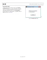
Power-Down Control 

Click the blue progressive disclosure button on the 

POWER-

DOWN LOGIC

 block to access the selection box, which allows 

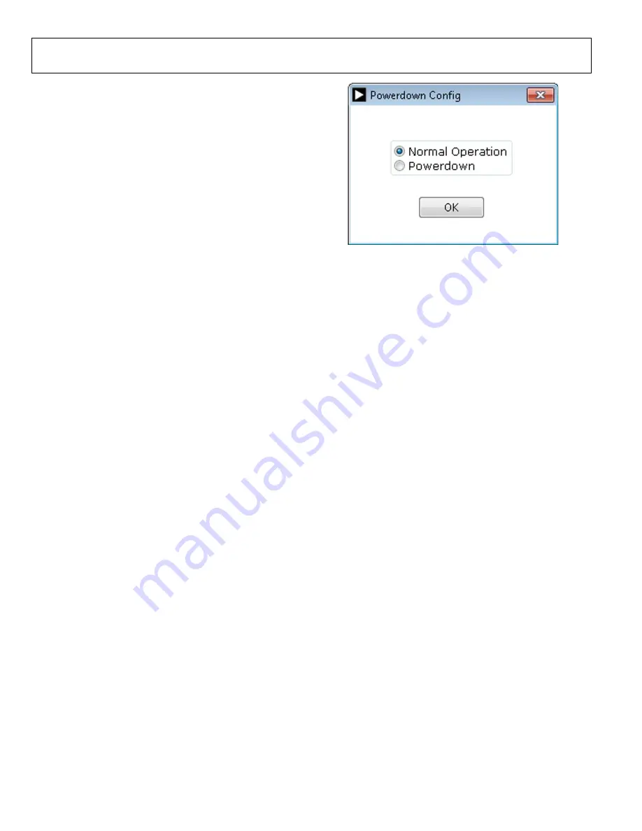
the device to operate in normal mode or power-down mode. A 
window opens that allows the user to click the 

Powerdown


option for the DAC, as shown in Figure 7. Click 

OK

 to write the 

appropriate values to the 

AD5340


Figure 7. 

Powerdown Config

 Window 


14516-

006

Summary of Contents for EVAL-AD5340DBZ

Page 1: ...tware HARDWARE REQUIRED EVAL SDP CB1Z board SDP B controller board must be purchased separately GENERAL DESCRIPTION This user guide details the operation of the evaluation board for the AD5340 single...

Page 2: ...ion History 2 Evaluation Board Hardware 3 Power Supplies 3 Link Options 3 Daughter Board Link Options 3 Evaluation Board Software Quick Start Procedures 4 Installing the Software 4 Running the Softwar...

Page 3: ...d Table 4 match the evaluation board imprints see Figure 12 Table 2 Link Options Setup for SDP B Control Default Link Number Position REF1 2 5V REF2 EXT REF3 EXT REF4 EXT LK5 C LK6 3V3 LK7 B DAUGHTER...

Page 4: ...d in the box 5 Proceed through any dialog boxes that appear to finalize the installation when the software detects the EVAL AD5340DBZ evaluation board RUNNING THE SOFTWARE To run the program complete...

Page 5: ...ressive disclosure button on the INTERFACE LOGIC block A window opens that allows the user to click the appropriate LDAC setting as shown in Figure 5 Figure 5 DAC Config Window GAIN Control Set the GA...

Page 6: ...he POWER DOWN LOGIC block to access the selection box which allows the device to operate in normal mode or power down mode A window opens that allows the user to click the Powerdown option for the DAC...

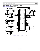
Page 7: ...EEPROM_A0 55 NC 54 NC 53 NC 52 GND 51 NC 50 NC 49 TMR_C 48 TMR_A 47 GPIO6 46 GND 45 GPIO4 44 GPIO2 43 GPIO0 42 SCL_1 41 SDA_1 40 GND 39 SPI_SEL1 SPI_SS 38 SPI_SEL_C 37 SPI_SEL_B 36 GND 35 SPORT_INT 34...

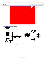
Page 8: ...I PMOD CONNNECTOR GPIO PMOD CONNNECTOR I2C PMOD CONNNECTOR 1 3 5 7 9 2 4 6 8 10 J2 1 2 3 4 5 6 7 8 9 10 11 12 13 14 15 16 J1 SDIN SDO SCLK SYNC SCL LDAC CLR PD GAIN SDA 1 2 3 4 5 6 7 8 J9 J8 1 J8 2 J8...

Page 9: ...EVAL AD5340DBZ User Guide UG 981 Rev 0 Page 9 of 13 Figure 12 EVAL MBnanoDAC SDZ Motherboard Component Placement Figure 13 EVAL MBnanoDAC SDZ Motherboard Top Side Routing 14516 012 14516 013...

Page 10: ...4 7 J4 8 1 2 3 4 5 6 7 8 9 10 11 12 13 14 15 16 J1 1 DB10 2 DB11 3 BUF 4 VREF 5 VOUT 6 NC 7 GND 8 9 10 11 12 13 14 VDD 15 DB0 16 DB1 17 DB2 18 DB3 19 DB4 20 DB5 21 DB6 22 DB7 23 DB8 24 DB9 U1 AD5340BR...

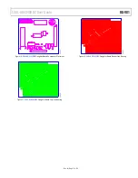
Page 11: ...81 Rev 0 Page 11 of 13 Figure 16 EVAL AD5340DBZ Daughter Board Component Placement Figure 17 EVAL AD5340DBZ Daughter Board Top Side Routing Figure 18 EVAL AD5340DBZ Daughter Board Bottom Side Routing...

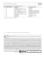
Page 12: ...FEC 1667509 1 J10 120 way connector FEC 1324660 1 L1 Inductor SMD 600 FEC 9526862 1 LK5 6 pin 3 2 0 1 inch header and shorting block FEC 148 535 and 150 411 36 pin strip 2 LK6 LK7 4 pin 2 2 0 1 inch...

Page 13: ...any entity other than ADI Customer their employees affiliates and in house consultants The Evaluation Board is NOT sold to Customer all rights not expressly granted herein including ownership of the...

Reviews: