


EVAL-ADAQ8088EBZ
User Guide
UG-1825
Rev. 0 | Page 3 of 12
EVALUATION BOARD HARDWARE
SETTING UP THE EVALUATION BOARD
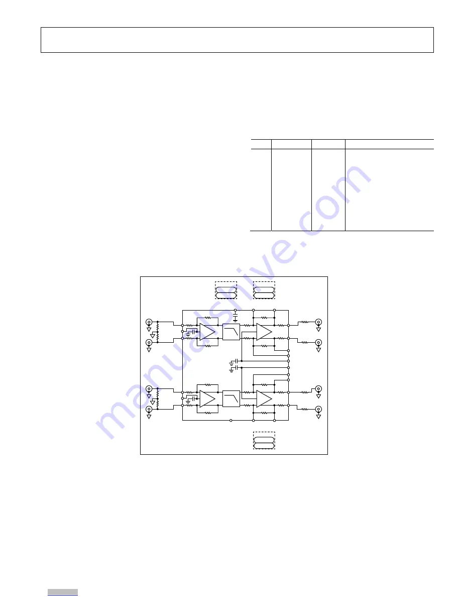
Figure 2 shows the simplified EVAL-ADAQ8088EBZ block
diagram. The ADAQ8088 μModule that is soldered to the
EVAL-ADAQ8088EBZ requires a supply voltage from 2.7 V to
3.3 V. The EVAL-ADAQ8088EBZ allows the user to set the
I_OUT_V
OCM
pin and Q_OUT_V
OCM
pin of the EVAL-
ADAQ8088EBZ through the EXVCMA and EXVCMB jumpers.
ANALOG INPUTS
The EVAL-ADAQ8088EBZ I inputs (I_INP and I_INN) are
connected through the J1 and J2 SMA connectors, respectively,
and the Q inputs (Q_INP and Q_INN) are connected through
the J4 and J3 SMA connectors, respectively.
Table 1. Jumper Details with Factory Default Settings
Link Default
Function Comment
P1
Not
populated
VS+ ADAQ8088
supply.
P2
Not
populated
EXVCMA
Connect EXVCMA to the
common-mode output of the
ADC I-channel. This jumper
can also be left floating.
P3
Not
populated
EXVCMB
Connect EXVCMB to the
common-mode output of the
ADC Q-channel. This jumper
can also be left floating.
Note that the I-channel and the Q-channel correspond to
Channel A and Channel B, respectively, of the ADAQ8088
data sheet.
Figure 2. Simplified EVAL-ADAQ8088EBZ Block Diagram
+
+
–
–
+
+
–
–
VCC I_OUT_RGP I_OUT_RFN
I_OUT_RFP
I_OUT_RGN
Q_OUT_RFP
Q_OUT_RGN
I_OUT_V
OCM
Q_OUT_V
OCM
Q_IN_V
OCM
J4
J3
+
+
–
–
+
+
–
–
Q_OUT_RGN Q_OUT_RFP
GND
J8
J6
J1
J2
Q_INP
Q_INN
I_INP
I_INN
Q_OUTP
Q_OUTN
I_OUTP
I_OUTN
J7
J5
EXVCMA
GND
P2
EXVCMB
GND
P3
VS+
GND
P1
25399-
002
Downloaded from
Downloaded from
Downloaded from


