background image

UG-669 

EVAL-ADuC7026 User Guide 


Rev. B | Page 4 of 16 

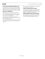
POWER INDICATOR/GENERAL-PURPOSE LEDS 

A power LED (D3) is used to indicate that a sufficient supply is 
available on the board. A general-purpose LED (D2) is directly 
connected to P4.2 of th

ADuC7026

. When P4.2 is cleared, the 

LED is turned on, and when P4.2 is set, the LED is turned off. 

ANALOG I/O CONNECTIONS 

All analog I/O connections are brought out on Header J3. 
ADC0 and ADC1 are buffered using a

AD8606

 to evaluate 

single-ended and pseudo differential mode. A potentiometer 
can be connected to ADC0 (buffered). 
ADC3 and ADC4 can be buffered with a single-ended to 
differential op amp on-board, with the 

AD8132

 used to evaluate 

the ADC in fully differential mode. 
ADC2 and ADC5 to ADC11 are not buffered. Be sure to follow 
the data sheet recommendations when connecting signals to 
these inputs. 

DAC1 can be used to control the brightness of the LED D1, 
when connected via the S1 switch. 

GENERAL-PURPOSE PROTOTYPE AREA 

General-purpose prototype areas are provided at the bottom  
of the evaluation board for adding external components as 
required in the user’s application. AV

DD

, AGND, V

DDIO

, and 

DGND tracks are provided in the prototype area. 

EXTERNAL MEMORY AND LATCH FOOTPRINT 

Footprints for a 32 k × 16 static RAM (CY7C1020CV33), a  
64 k × 16 flash (AT29LV1024), and a16-bit latch are also  
on board. See the External Memory Interface section. 


Summary of Contents for EVAL-ADuC7026

Page 1: ...e code QUICKSTART PLUS DEVELOPMENT SYSTEM KIT CONTENTS ADuC7026 evaluation board mIDAS Link JTAG emulator USB cable Serial download cable International power supply CD containing evaluation software ADuC7026 data sheet example code GENERAL DESCRIPTION This user guide which replaces AN 744 refers to revision B2 of the ADuC7026 MicroConverter evaluation boards Two models of the development kit are a...

Page 2: ... Options 5 S1 1 VREF 5 S1 2 VOCM 5 S1 3 POT 5 S1 4 ADC3 5 S1 5 VIN 5 S1 6 VIN 5 S1 7 ADC4 5 S1 8 LED 5 External Connectors 6 Analog I O Connector J3 6 Power Supply Connector J5 6 Emulation Connector J4 6 Serial Interface Connector J1 6 Digital I O Connector J2 6 External Memory Interface 8 Connections 8 Potentiometer Demonstration Circuit 10 Schematic and Artwork 11 Bill of Materials 13 REVISION H...

Page 3: ...r to the J4 connector CRYSTAL CIRCUIT The board is fitted with a 32 768 kHz crystal from which the on chip PLL circuit can generate a 41 78 MHz clock EXTERNAL REFERENCE ADR291 The external 2 5 V Reference Chip U2 has two functions It is provided on the evaluation board to demonstrate the external reference option of the ADuC7026 but its main purpose is to generate the VOCM voltage of the different...

Page 4: ...ered with a single ended to differential op amp on board with the AD8132 used to evaluate the ADC in fully differential mode ADC2 and ADC5 to ADC11 are not buffered Be sure to follow the data sheet recommendations when connecting signals to these inputs DAC1 can be used to control the brightness of the LED D1 when connected via the S1 switch GENERAL PURPOSE PROTOTYPE AREA General purpose prototype...

Page 5: ...t on Header J3 S1 4 ADC3 Function Brings out ADC3 Pin 80 on Header J3 Use Slide S1 4 to the on position to connect ADC3 of Header J3 directly to the ADC3 pin Pin 80 of the ADuC7026 Slide S1 4 to the off position to disconnect ADC3 of Header J3 from the ADC3 pin Pin 80 of the ADuC7026 S1 5 VIN Function Connects the OUT pin of the single ended to differential op amp AD8132 to ADC3 S1 5 and S1 6 must...

Page 6: ...DAS link provided in the ADuC7026 QuickStart Plus development system only SERIAL INTERFACE CONNECTOR J1 Connector J1 provides a simple connection of the evaluation board to the PC via a PC serial port cable provided with the ADuC7026 development system DIGITAL I O CONNECTOR J2 Connector J2 provides external connections for all GPIOs The pinout of the connector is shown in Table 3 Table 2 Pin Funct...

Page 7: ... RS PLAO 7 J2 17 P2 1 PWM0H WS PLAO 6 J2 18 P2 7 PWM1L MS3 J2 19 P3 7 PWMSYNC AD7 PLAI 15 J2 20 P3 6 PWMTRIP AD6 PLAI 14 J2 21 P0 7 ECLK XCLK SIN PLAO 4 Pin No Pin Description J2 22 P2 0 CONVSTART SOUT PLAO 5 J2 23 P0 5 IRQ1 ADCBUSY MS0 PLAO 2 J2 24 P0 4 IRQ0 PWMTRIP MS1 PLAO 1 J2 25 P3 5 PWM2L AD5 PLAI 13 J2 26 P3 4 PWM2H AD4 PLAI 12 J2 27 P2 6 PWM1H MS2 J2 28 P2 5 PWM0L MS1 J2 29 P0 3 TRST A16 A...

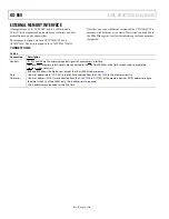
Page 8: ...g to slower memory if required CONNECTIONS Table 4 Connection Description Controls RS WS and AE are the minimum control signals of any memory interface MS0 and MS1 memory select signals are connected to the CE of the SRAM and the flash respectively to enable the memory when necessary BHE and BLE allows the high or low byte of the 16 bit SRAM to be selected Data 16 bits of address data AD 15 0 are ...

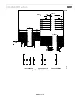
Page 9: ... GND 4 GND U7 74LVT16373ADGG C25 0 1µF C26 0 1µF C27 0 1µF C28 0 1µF C29 0 1µF C30 0 1µF 2 A0 3 A1 4 A2 5 A3 6 A4 7 A5 9 A6 10 A7 11 A8 12 VSS 13 A9 14 A10 15 A11 17 A12 18 A13 19 A14 20 A15 22 WE 23 VCC 27 CE 28 O15 29 O14 30 O13 31 O12 32 O11 34 O10 35 O9 36 O8 37 VSS 38 O7 39 O6 40 O5 42 O4 43 O3 44 O2 45 O1 46 O0 47 OE U6 AT29LV1024 C31 0 1µF R23 0Ω AD 0 15 VDDIO ADR 0 15 ADR0 ADR1 ADR2 ADR3 A...

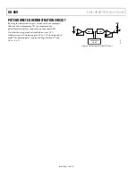
Page 10: ...ccompanying CD the variation in the potentiometer resistance can be seen on the output LED Note that the internal and external reference are 2 5 V which gives an ADC input range of 0 V to 2 5 V in single ended mode The potentiometer can give a voltage between 0 V and AVDD 3 3 V AVDD AVDD APPLICATION CODE DAC ADC 05032 003 Figure 4 Circuit Diagram of the RTD Circuit ...

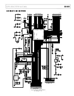
Page 11: ...20 270Ω R19 1 5Ω C7 22pF D4 R15 1kΩ R14 0Ω 3 2 1 U4 A AD8606ARZ 5 6 7 U4 B AD8606ARZ 8 V 4 V U4 C 8 IN 2 VOCM 1 IN 5 OUT 4 OUT 6 V 3 V U3 AD8132 R10 60 4Ω R11 60 4Ω C8 22pF R5 348Ω R6 348Ω R9 348Ω R8 348Ω C4 0 1µF C11 470nF R22 100kΩ R21 100kΩ R18 270Ω C12 0 1µF D1 R12 270Ω R13 0Ω CW R1 C2 0 1µF R2 100Ω R3 200Ω 1 2 3 4 5 6 7 8 9 10 11 12 13 14 15 16 S1 SW8DIP S2 2 VIN 5 TRIM 6 VOUT 4 GND U2 ADR291...

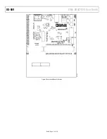
Page 12: ...UG 669 EVAL ADuC7026 User Guide Rev B Page 12 of 16 05032 005 Figure 6 Evaluation Board Silkscreen ...

Page 13: ... 005 Farnell C9 C10 2 10 nF Surface mount ceramic capacitor 0603 case 301 9561 Farnell C11 C19 2 470 nF Surface mount ceramic capacitor 0603 case 318 8851 Farnell C20 C21 2 12 pF Surface mount ceramic capacitor 0603 case 721 979 Farnell R1 1 10 kΩ potentiometer 0 25W 4 series 4 mm 4 mm square TS53YJ 10K 20 TR lead free Vishay R2 1 100 Ω Surface mount resistor 0603 case 933 2375 Farnell R3 1 200 Ω ...

Page 14: ...UG 669 EVAL ADuC7026 User Guide Rev B Page 14 of 16 NOTES ...

Page 15: ...EVAL ADuC7026 User Guide UG 669 Rev B Page 15 of 16 NOTES ...

Page 16: ...for any reason Upon discontinuation of use of the Evaluation Board or termination of this Agreement Customer agrees to promptly return the Evaluation Board to ADI ADDITIONAL RESTRICTIONS Customer may not disassemble decompile or reverse engineer chips on the Evaluation Board Customer shall inform ADI of any occurred damages or any modifications or alterations it makes to the Evaluation Board inclu...

Reviews: