background image

HSC-ADC-EVALC 


Rev. 0 | Page 4 of 32 

EVALUATION BOARD HARDWARE

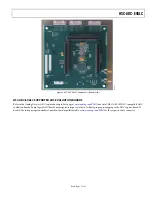
HSC-ADC-EVALC ADC CAPTURE BOARD  

EASY 

START 

Requirements 


HSC-ADC-EVALC ADC capture board, VisualAnalog, 5 V 

wall transformer, and USB cable 


High speed ADC evaluation board and ADC data sheet 


Power supply for ADC evaluation board 


Analog signal source and appropriate filtering 


Low jitter clock source applicable for specific ADC 

evaluation, typically <1 ps rms jitter 


PC running Windows® 98 (2nd edition), Windows 2000, 

Windows ME, or Windows XP 


PC with a USB 2.0 port recommended (USB 1.1 compatible)  

Easy Start Steps 

Important Note 

Administrative rights for the Windows operating systems are 
needed during the entire easy start procedure.  

Completion of every step before reverting to a normal user 
mode is recommended. 

1.


Install VisualAnalog from the CD provided in the ADC 
capture board kit or download the latest version from the 
Web. For the latest updates to the software, check the 
Analog Devices website at 

www.analog.com/FIFO

2.


Connect the ADC capture board to the ADC evaluation 
board. If an adapter is required, insert the adapter between 
the ADC evaluation board and the ADC capture board.  

3.


Connect the provided USB cable to the ADC capture board 
and to an available USB port on the computer. 

4.


Refer to Table 1 for setting the ADC capture board’s I/O 
logic level to match the level coming from the ADC evalua-
tion board. 1.8 V is default; 2.5 V and 3.3 V are jumper 
selectable. Most evaluation boards can be used with the 
default settings. 

5.


The ADC capture board is supplied with a wall mount 
switching power supply. Connect the supply end to an ac 
wall outlet rated for 100 Vac to 240 Vac at 47 Hz to 63 Hz. 
The other end is a 2.1 mm inner diameter jack that connects 
to the PCB at J4.  

6.


Once the USB cable is connected to both the computer and 
the HSC-ADC-EVALC board, and power is applied, the 
USB driver starts to install. The 

Found New Hardware


Wizard

 opens and prompts you through the automated 

install process.  

7.


(Optional) Verify in the Windows device manager that 

Analog


Devices ADC-HSC-EVALC

 is listed under the 

USB hardware. 

8.


Refer to the instructions included in the respective ADC 
data sheet found at 

www.analog.com/FIFO

 for more 

information about connecting the ADC evaluation board’s 
power supply and other requirements. After verification of 
power supply connections, apply power to the ADC 
evaluation board and check the voltage levels on the ADC 
board to make sure they are correct. 

9.


Make sure the evaluation boards are powered on before 
connecting the analog input and clock. Connect the 
appropriate analog input (which should be filtered with a 
band-pass filter) and low jitter clock signal.  

10.


Refer to the 

VisualAnalog User Manual

 at 

www.analog.com/FIFO

 for detailed software operating 

instructions. 

POWER SUPPLIES 

The ADC capture board is supplied with a wall mount switch-
ing power supply that provides a 5 V, 3 A maximum output. 
Connect the supply to the rated 100 Vac to 240 Vac wall outlet at 
47 Hz to 63 Hz. The other end is a 2.1 mm inner diameter jack 
that connects to the PCB at J4. On the PC board, the supply is 
fused and conditioned before connecting to the regulators that 
supply the proper bias to the entire ADC capture board. 

CONNECTION AND SETUP 

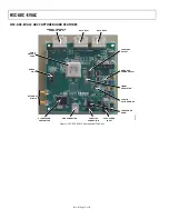
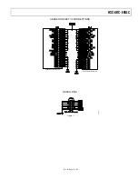
The ADC capture board has two 40-pin connectors (J2 and J3) 
that accept two 18-bit channels of parallel CMOS or LVDS 
inputs from the ADC (see Figure 

2

). The third 40-pin connector 

(J1) is used to pass SPI and other USB/FPGA control signals 
across to adjacent ADC evaluation boards that support these 
features. 


Summary of Contents for HSC-ADC-EVALC

Page 1: ...jitter clock source High speed ADC evaluation board and ADC data sheet PC running Windows 98 2nd edition Windows 2000 Windows ME or Windows XP Latest version of VisualAnalog USB 2 0 port recommended U...

Page 2: ...Setup 4 Jumpers 5 HSC ADC EVALC ADC Capture Board Features 6 HSC ADC EVALC Supported ADC Evaluation Boards 7 Theory of Operation 8 Configuration 8 Input Circuitry 8 Data Capture 8 Code Description 8...

Page 3: ...re digital data at speeds up to 644 MSPS single data rate SDR and 800 MSPS double data rate DDR The FPGA contains an integrated FIFO memory that allows capture of data record lengths up to a total of...

Page 4: ...e other end is a 2 1 mm inner diameter jack that connects to the PCB at J4 6 Once the USB cable is connected to both the computer and the HSC ADC EVALC board and power is applied the USB driver starts...

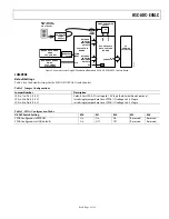
Page 5: ...Using ADC Evaluation Board and HSC ADC EVALC ADC Capture Board JUMPERS Default Settings Table 1 lists the default settings for the HSC ADC EVALC evaluation kit Table 1 Jumper Configurations Jumper Num...

Page 6: ...O USB SPI CONTROL DATA BUS 1 DATA BUS 2 FPGA LOAD SELECT ON BOARD POWER SUPPLY 100MHz OSCILLATOR FPGA I O VOLTAGE MODE FPGA CONFIG PROM XILINX VIRTEX 4 FPGA DEBUG PINS EXTERNAL SYNC I O CYPRESS USB CO...

Page 7: ...ces ADC capture board product page at www analog com FIFO for a list of HSC ADC EVALC compatible ADC evaluation boards Some legacy ADC boards may require interposer cards to facilitate proper pin mapp...

Page 8: ...or 3 3 V logic levels and can accept LVDS or CMOS inputs Each channel of the ADC capture board requires a clock signal to capture data These clock signals are normally provided by the attached ADC eva...

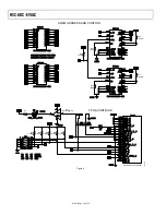
Page 9: ...f 32 EVALUATION BOARD SCHEMATICS AND ARTWORK HSC ADC EVALC SCHEMATICS 06676 005 TYCO AND DSP EZ KIT CONNECTOR TO FPGA XC4VFX20 10FFG672C XC4VFX20 10FFG672C XC4VFX20 10FFG672C XC4VFX20 10FFG672C R38 10...

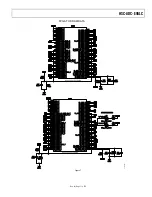
Page 10: ...Rev 0 Page 10 of 32 06676 006 SRAM ADDRESS AND CONTROL FPGA CONTROLS U21 NC7SZ05M5X R1 100 R40 3 74K R44 3 74K R42 3 74K R41 3 74K R43 3 74K XC4VFX20 10FFG672C R28 3 74K R27 249 R33 249 R25 3 74K R31...

Page 11: ...HSC ADC EVALC Rev 0 Page 11 of 32 FPGA TO SRAM DATA XC4VFX20 10FFG672C 06676 007 XC4VFX20 10FFG672C Figure 7...

Page 12: ...HSC ADC EVALC Rev 0 Page 12 of 32 AD19 TO BE USED WITH HIGHER DENSITY SRAM DEVICES 06676 008 Figure 8...

Page 13: ...HSC ADC EVALC Rev 0 Page 13 of 32 SRAM AND FPGA POWER 06676 009 XC4VFX20 10FFG672C XC4VFX20 10FFG672C R66 499 R64 499 R65 499 R63 499 Figure 9...

Page 14: ...HSC ADC EVALC Rev 0 Page 14 of 32 06676 010 REFCLK Oscillator for IDELAYCTRL FPGA BYPASS CAP SRAM A BYPASS CAP SRAM B BYPASS CAP R15 24 Figure 10...

Page 15: ...HSC ADC EVALC Rev 0 Page 15 of 32 06676 011 DEBUG PINS UNUSED ROCKET I 0 CONNECTIONS XC4VFX20 10FFG672C XC4VFX20 10FFG672C Figure 11...

Page 16: ...HSC ADC EVALC Rev 0 Page 16 of 32 06676 012 ROCKET I 0 CONNECTIONS Figure 12...

Page 17: ...HSC ADC EVALC Rev 0 Page 17 of 32 06676 013 USB CONNECTIONS R49 3 74 R71 3 74 R48 100K SDI SDO DIRECTIONS ARE WITH RESPECT TO THE DEVICE UNDER CONTROL USB Direct I O 3 3V Figure 13...

Page 18: ...HSC ADC EVALC Rev 0 Page 18 of 32 USB CONNECTIONS CONTINUED 06676 014 4 5 2 1 3 6 R52 3 74K R72 3 74K R46 499 XC4VFX20 10FFG672C XC4VFX20 10FFG672C J6 Figure 14...

Page 19: ...HSC ADC EVALC Rev 0 Page 19 of 32 06676 015 EZ KIT EXPANSION INTERFACE FOR DSPs P1 P2 P3 Figure 15...

Page 20: ...HSC ADC EVALC Rev 0 Page 20 of 32 06676 016 TYCO HM Zd CONNECTORS J1 HS SERIAL SPI AUX J2 DATA BUS 1 J3 DATA BUS 2 Figure 16...

Page 21: ...HSC ADC EVALC Rev 0 Page 21 of 32 06676 017 CONFIGURATION EEPROM JTAG CONNECTOR EEPROM HARDWARE RECONFIGURATION PUSHBUTTON R57 3 74K R73 ZERO R77 100 R78 100 R75 3 74K R76 3 74K Figure 17...

Page 22: ...HSC ADC EVALC Rev 0 Page 22 of 32 POWER AND VOLTAGE REGULATORS 06676 018 TSW 102 08 G D DO NOT REMOVE R68 147k Figure 18...

Page 23: ...S 1 DATA BUS 2 XILINX VIRTEX 4 FPGA DEBUG PINS EXTERNAL SYNC I O CYPRESS USB CONTROLLER USB CONNECTOR FPGA JTAG CONNECTOR 5VDC POWER INPUT FPGA LOAD SELECT ON BOARD POWER SUPPLY 100MHz OSCILLATOR FPGA...

Page 24: ...1A D9A D7A D5A D3A D1A DCLKA2 DCLKA1 D15A D13A D11A D9A D7A D5A D3A D1A DCLKA2 LVDS DATA PATH CMOS LVDS DATA PATH LVDS DATA PATH CMOS LVDS DATA PATH D17B D16B D14B D12B D10B D8B D6B D4B D2B D0B D17B D...

Page 25: ...O_6 I O_8 CSB_1 CSB_2 CSB_3 CSB_4 USB_3 USB_5 J1 HS SERIAL SPI AUX HIGH SPEED SERIAL REFERENCE CLK HIGH SPEED SERIAL DATA INPUTS FUTURE HIGH SPEED SERIAL DATA INPUTS FPGA GENERAL PURPOSE I O SPI CONT...

Page 26: ...D7 SD3 AD1 A8 I O_6 AA3 B8 I O_5 Y3 C8 SD2 G1 D8 SD2 H1 A9 I O_4 W3 B9 I O_3 V3 C9 SD1 A4 D9 SD1 A3 A10 I O_2 P3 B10 I O_1 N3 C10 MGTCLK1 K1 D10 MGTCLK1 L1 Table 4 HSC ADC EVALC J2 I O Connections to...

Page 27: ...H9 B2 D1A G9 C2 D2A E8 D2 D2A E7 A3 D3A L10 B3 D3A L9 C3 D4A J9 D3 D4A K10 A4 D5A C3 B4 D5A D3 C4 D6A E3 D4 D6A F3 A5 D7A D5 B5 D7A E5 C5 D8A C4 D5 D8A D4 A6 D9A B7 B6 D9A C7 C6 D10A B6 D6 D10A C6 A7...

Page 28: ...MD AVX TPSC106K025R0500 2 C47 C51 Capacitor 47 F 10 V tantalum TEL SMD Epcos Inc B45197A2476K309 2 C49 C50 Capacitor 1000 pF 50 V ceramic Y5V 0402 Panasonic ECG ECJ 0EF1H102Z 17 C5 C19 C23 C24 C31 C53...

Page 29: ...5 0402 SMD Panasonic ECG ERJ 2GE0R00X 2 R53 R70 Resistor 80 6 k 1 16 W 1 0402 SMD Panasonic ECG ERJ 2RKF8062X 1 R54 Resistor low value 1206 SMD 0 04 TT Electronics LRC LR1206LF 01 R040 F 1 R55 Resisto...

Page 30: ...ences SOT 23 RT 3 do not install Analog Devices ADR512ART 0 R9 Resistor 6 2 k 1 16 W 5 0402 SMD do not install Panasonic ECG ERJ 2GEJ622X 0 R12 R13 R14 R51 Resistor 0 1 16 W 5 0402 SMD do not install...

Page 31: ...HSC ADC EVALC Rev 0 Page 31 of 32 NOTES...

Page 32: ...HSC ADC EVALC Rev 0 Page 32 of 32 NOTES 2007 Analog Devices Inc All rights reserved Trademarks and registered trademarks are the property of their respective owners EB06676 0 4 07 0...

Reviews: