1
dc2234af
DEMO MANUAL DC2234A
Description
LT8711
Micropower Synchronous
Sepic Converter
Demonstration circuit 2234A is a synchronous sepic
converter featuring the
LT
®
8711
multitopology switching
controller. The LT8711 is a current mode PWM DC/DC
controller with a dual input LDO to optimize gate driver
efficiency. Ultralow 15μA quiescent current in low noise
Burst Mode
®
operation achieves high efficiency at very
light loads and helps extend the run-time in battery pow-
ered applications when in standby mode. The LT8711
switching frequency can be programmed either via oscil-
lator resistor or external clock over a 100kHz to 750kHz
range.
The demo board regulates a 12V, 4A output from a 4.5V
to 40V input source, and operates at 200kHz switching
frequency. The rated maximum load current is 4A, while
derating is necessary for certain input voltage and thermal
conditions.
The SYNC pin on the demo board is grounded (JP1 at
BURST position) by default for low ripple high efficiency
Burst Mode operation at light load. To synchronize to an
external clock, move JP1 to SYNC and apply the external
clock to the SYNC turret. Force continuous conduction
mode can be selected by moving JP1 shunt to FCM posi-
tion.
L
, LT, LTC, LTM, Linear Technology, Burst Mode and the Linear logo are registered trademarks
of Analog Devices, Inc. All other trademarks are the property of their respective owners.
performance summary
The DC2234A can be modified from a SEPIC converter to
other topologies. Synchronous BOOST and some other
schematics are provided in the data sheet. Please consult
the factory or LT8711 data sheet for details regarding
how to customize the DC2234A or how to design different
topologies for custom specifications.
The LT8711 includes many other features such as user
configurable under voltage lockout, soft-start, input volt-
age feedforward regulation, and it is easily configured
as synchronous buck, boost, SEPIC or nonsynchronous
buck-boost converter.
The data sheet gives a complete description of the device,
operation and application information. The data sheet
must be read in conjunction with this demo manual for
DC2234A. The LT8711 is assembled in a 20-lead plastic
TSSOP package with a thermally enhanced ground pad.
Proper board layout is essential for maximum thermal
performance. See the Layout Considerations section in
the data sheet.
Design files for this circuit board are available at
http://www.linear.com/demo/DC2234A
Specifications are at T
A
= 25°C
SYMBOL
PARAMETER
CONDITIONS
MIN
TYP
MAX
UNITS
V
IN
Input Voltage Range
4.5
40
V
V
OUT
Output Voltage
11.6
12
12.4
V
I
OUT
Maximum Output Current
Derating is Necessary for Certain V
IN
and
Thermal Conditions
4
A
t
SW
Switching Frequency
185
200
215
kHz
EFF
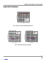
Efficiency at DC
V
IN
= 5V, I
OUT
= 1A
V
IN
= 12V, I
OUT
= 2A
V
IN
= 24V, I
OUT
= 4A
V
IN
= 36V, I
OUT
= 4A
91.9
92
91.4
90.2
%
%
%
%
Downloaded from


