background image

2

DEMO MANUAL 

DC2824A-A

Rev. 0

QUICK START PROCEDURE

Demonstration circuit 2824A-A is easy to set up to evalu-

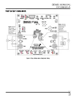
ate the performance of the LTC7131-1. Refer to Figure 1 

for the proper measurement equipment setup and follow 

the procedure below. 
1.  With power off, connect the input power supply to 

V

IN

 (4.5V to 20V) and GND (input return). Make sure 

the input power supply is capable of 25A at 4.5V 

(to satisfy the power requirement at 4V out with 

25A load).

2.  Connect the 1V output load between V

OUT

 and GND 

(Initial load: no load).

3.  Connect the DVMs to the input and outputs. Set 

default jumper position:  RUN_MSTR(JP1):  ON; 

RUN_STBY(JP3): ON; MODE(JP2): FCM; 

MARGIN  (JP4): NOM; ILIM(JP9):  25A; V

OUT


SEL: JP6. WP(JP5): OFF.  

4.  Turn on the input power supply and check for the 

proper output voltages. V

OUT

 should be 1V ± 0.5%.

5.  Once the proper output voltage is established, adjust 

the load within the operating range and observe 

the output voltage regulation, ripple voltage and 

other parameters.

6.  Connect the dongle and control the output voltage 

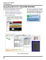
from the GUI. See LTpowerPlay for LTC7131-1 Quick 

Start Procedure section for details.

PERFORMANCE SUMMARY

Specifications are at T

A

 = 25°C

PARAMETER

CONDITIONS

MIN

TYP

MAX

UNITS

Input Voltage Range

4.5

12

20

V

Output Voltage, V

OUT

V

IN

 = 4.5V to 20V, I

OUT

 = 0A to 25A

0.4

1

4

V

Maximum Output Current, I

OUT

V

IN

 = 4.5V to 20V, V

OUT

 = 0.4V to 4V

25

A

Typical Efficiency

V

IN

 =12V, V

OUT

 = 1V, I

OUT

 = 25A, f

SW

 = 480kHz

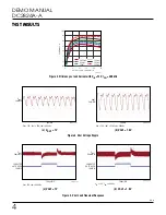
87.7 (See Figure 3)

%

V

IN

 =12V, V

OUT

 = 1.8V, I

OUT

 = 25A, f

SW

 = 480kHz

91.4 (See Figure 3)

%

Default Switching Frequency

480

kHz


Notes


1.  When measuring the output or input voltage 

ripple, do not use the long ground lead on the 

oscilloscope probe. See Figure 1 for the proper 

scope probe technique. Short, stiff leads need 

to be soldered to the (+) and (−) terminals of an 

output capacitor. The probe’s ground ring needs 

to touch the (−) lead and the probe tip needs to 

touch the (+) lead. 


+

V

OUT

GND

C

OUT

Figure 1. Measuring Output Voltage Ripple


  A BNC test terminal (J5) is also implemented on 

board to measure output voltage and its ripple 

for the convenience of evaluation.


2.  The default 215nH inductor installed on this 

demo board is chosen based on 1V and 1.8V 

output at 480kHz default switching frequency. 

However, when changing the output voltage and/

or switching frequency, please determine if the 

inductance is still suitable by calculating the 

peak-peak inductor current ripple and make sure 

it stays at 30% to 50% of load current. Refer 

to the Inductor Selection section of LTC7131-1 

data sheet for more information. 

Summary of Contents for LTC7131-1

Page 1: ...er To fully explore the extensive power system manage ment features of the part download the GUI software LTpowerPlay onto your PC and use ADI s USB to PMBus dongle DC1613A to connect to the board All registered trademarks and trademarks are the property of their respective owners BOARD PHOTO LTpowerPlay allows users to monitor fault status and real time telemetry of input and output voltages inpu...

Page 2: ...25 C PARAMETER CONDITIONS MIN TYP MAX UNITS Input Voltage Range 4 5 12 20 V Output Voltage VOUT VIN 4 5V to 20V IOUT 0A to 25A 0 4 1 4 V Maximum Output Current IOUT VIN 4 5V to 20V VOUT 0 4V to 4V 25 A Typical Efficiency VIN 12V VOUT 1V IOUT 25A fSW 480kHz 87 7 See Figure 3 VIN 12V VOUT 1 8V IOUT 25A fSW 480kHz 91 4 See Figure 3 Default Switching Frequency 480 kHz Notes 1 When measuring the output...

Page 3: ...3 DEMO MANUAL DC2824A A Rev 0 TEST SETUP DIAGRAM Figure 2 Proper Measurement Equipment Setup ...

Page 4: ... 95 100 EFFICIENCY dc2824a a F01 0 65VOUT 0 8VOUT 1VOUT 1 2VOUT 1 8VOUT 3 3VOUT 2µs DIV dc2824a a G04a VOUT 5mV DIV VIN 12V IOUT 25A fSW 480kHz a VOUT 1V 2µs DIV dc2824a a G04b VOUT 5mV DIV VIN 12V IOUT 25A fSW 480kHz b VOUT 1 8V 100µs DIV dc2824a a G05a VOUT 20mV DIV VIN 12V fSW 480kHz LOAD STEP 0A TO 6 25A 10A DIV a VOUT 1V 100µs DIV dc2824a a G05b VOUT 20mV DIV VIN 12V fSW 480kHz LOAD STEP 0A T...

Page 5: ... a demo board sys tem LTpowerPlay can also be used in an off line mode with no hardware present in order to build a multichip configuration file that can be saved and reloaded at a later time LTpowerPlay provides unprecedented diagnostic and debug features It becomes a valuable diagnostic tool during board bring up to program or tweak the power management scheme in a system or to diagnose power is...

Page 6: ...r laptop through the DC1613A dongle 3 Launch the LTpowerPlay GUI a The GUI should automatically identify the dongle connected as shown in the picture below Select Detect Chips to allow LTpowerPlay to detect the LTC7131 1 b After LTC7131 1 is detected the LTpowerPlay main interface appears as shown in Figure 7 and a message box like below also shows for a few seconds in the lower left hand corner c...

Page 7: ...ing the fault response modes e Here is an example of margining the output volt age high First enter the desired margin high percentage 25 in the MFR_VOUT_MARGIN_ HIGH field under Output Voltage tab Note that the percentage must be within the range of 25 to 25 for both margin high and mar gin low commands f Then select the MarginHigh operation from the On off Control and Margining tab g Next click ...

Page 8: ...R 0603 WURTH ELEKTRONIK 150060RS75000 17 1 D3 DIODE SCHOTTKY 30V 100mA SOD 323 CENTRAL SEMI CMHSH 3 TR 18 4 J2 J6 J8 EVAL BOARD STUD HARDWARE SET 10 32 ANALOG DEVICES 720 0010 19 1 L1 IND 215nH PWR FERRITE 10 61A 0 29mΩ 10 4mm 8 0mm SMD EATON FP1007R3 R22 R 20 1 Q1 XSTR MOSFET P CH 20V 5 9A TO 236 SOT23 3 VISHAY Si2365EDS T1 GE3 21 1 Q2 XSTR MOSFET N CH 60V 300mA SOT 23 VISHAY 2N7002K T1 GE3 22 1 ...

Page 9: ... MAX 2501 2 00 80 00 00 07 0 2 1 J1 CONN SHROUDED HDR MALE 2 6 2mm VERT STR THT AMPHENOL 98414 G06 12ULF 3 1 J3 CONN HDR MALE 2 4 2mm R A THT MOLEX 87760 0816 4 1 J4 CONN HDR FEMALE 2 4 2mm R A THT SULLINS CONNECTOR SOLUTIONS NPPN042FJFN RC 5 2 J5 J9 CONN RF BNC RCPT JACK 5 PIN STR THT 50Ω AMPHENOL RF 112404 6 3 JP1 JP3 JP5 CONN HDR MALE 1x3 2mm VERT STR THT NO SUBS ALLOWED WURTH ELEKTRONIK 620003...

Page 10: ...REV02 N A CONVERTER WITH PMBUS INTERFACE Monday June 14 2021 D A T E S H E E T O F T I T L E S C H E M A T I C A P P R O V A L S P C B D E S A P P E N G S I Z E S C H E M A T I C N O A N D R E V I S I O N C U S T O M E R N O T I C E T H I S C I R C U I T I S P R O P R I E T A R Y T O A N A L O G D E V I C E S A N D S U P P L I E D F O R U S E W I T H A N A L O G D E V I C E S P A R T S w w w a n a...

Page 11: ...G N A C I R C U I T T H A T M E E T S C U S T O M E R S U P P L I E D S P E C I F I C A T I O N S H O W E V E R I T R E M A I N S T H E C U S T O M E R S R E S P O N S I B I L I T Y T O V E R I F Y P R O P E R A N D R E L I A B L E O P E R A T I O N I N T H E A C T U A L A P P L I C A T I O N C O M P O N E N T S U B S T I T U T I O N A N D P R I N T E D C I R C U I T B O A R D L A Y O U T M A Y S ...

Page 12: ... disclose or transfer any portion of the Evaluation Board to any other party for any reason Upon discontinuation of use of the Evaluation Board or termination of this Agreement Customer agrees to promptly return the Evaluation Board to ADI ADDITIONAL RESTRICTIONS Customer may not disassemble decompile or reverse engineer chips on the Evaluation Board Customer shall inform ADI of any occurred damag...

Page 13: ...Mouser Electronics Authorized Distributor Click to View Pricing Inventory Delivery Lifecycle Information Analog Devices Inc DC2824A A ...

Reviews: