SSM2304
Rev. 0 | Page 16 of 20
061
62
-0
73
When differential mode audio signals are used as the input
signal source, either use Headers 3HD1 and 3HD2 or the
soldering pads located on the left side of the board and turn
Switches S1E and S1F to the off position (lower position). The
top header is for the left channel signals and the lower is for the
right channel signals. There are two ground soldering pads on
the lower left corner.
The lower side of the board has a switch bank and its corres-
ponding channels are listed in Table 5
Table 5. Switch Channels
Switch Name
Corresponding Channel
S1A Left
positive
S1B Left
negative
S1C Right
negative
S1D Right
positive
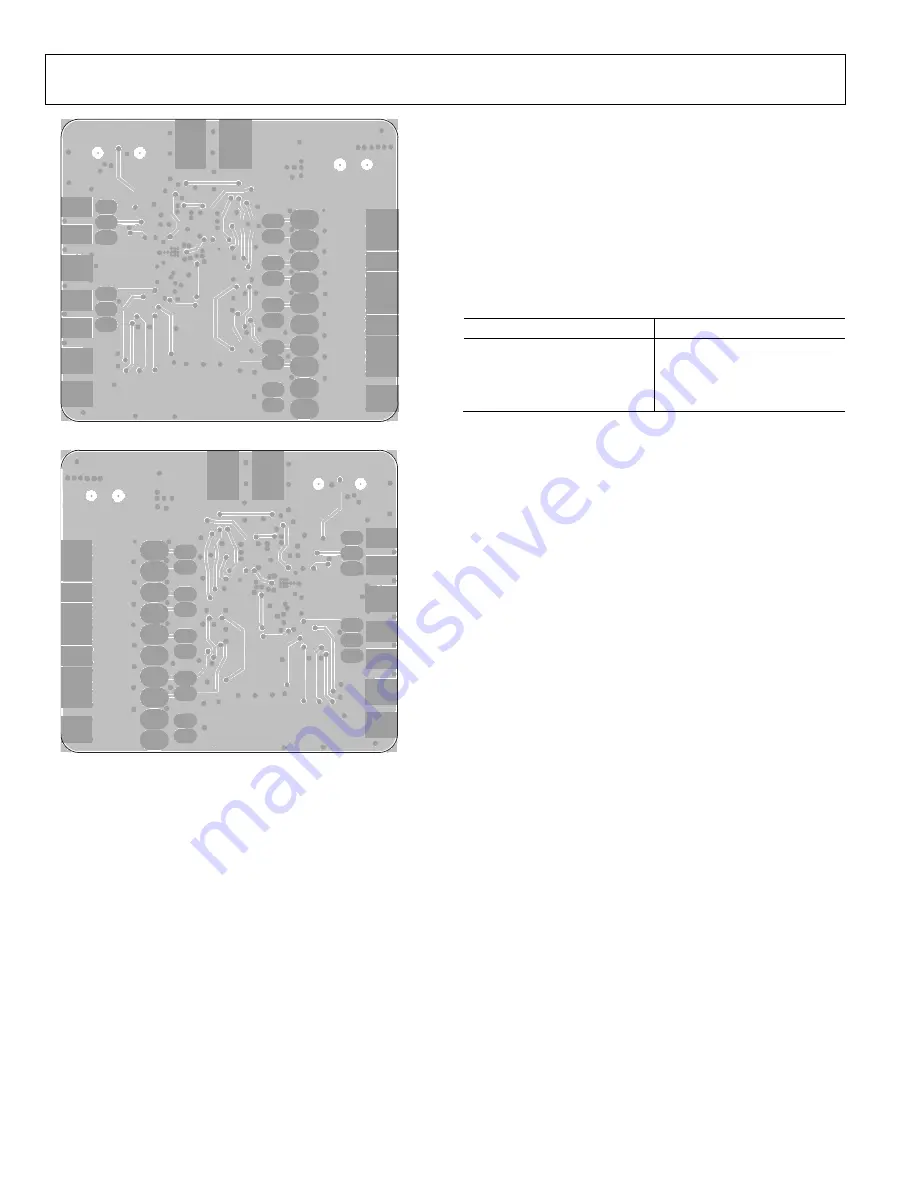
Figure 44. Bottom Layers
When the switches listed in Table 5 are placed in the upper
positions, their corresponding coupling capacitors are shorted;
when the switches are placed in the lower positions, the coupling
capacitors are inserted in the signal paths.
061
62
-0
74
As previously described, Switches S1E and S1F are used to ac
short circuit the left and right channel negative input ports to
ground, respectively. This function is only needed when driving
the input ports in single-ended mode. After shortening the
negative input ports to ground, the noise picked up by the input
port connections will be conducted to the ground.
S1G is not connected for the SSM2304.
S1H controls the shutdown function. The upper position shuts
down the amplifier, and the lower position turns on the amplifier.
The upper right corner has a dc power jack connector. The
center pin is for the positive terminal. It is compatible with 3 V
to 5 V voltage, and the maximum peak current is approximately
1.2 A when driving a 4 Ω load (for SSM2304 only) and 0.6 A
when driving an 8 Ω load with an input voltage of 5 V.
Figure 45. Mirrored Bottom Layers
On the upper left corner of the schematic shown in Figure 46,
there is an audio stereo jack connector (3.5 mm), J1. This jack is
compatible with standard stereo audio signals. It uses a
conventional audio stereo signal connector/cable to obtain
audio signals from common appliances, such as DVD players,
personal computers, TVs, and so on. Because this connector
only provides single-ended audio signals, turn Switches S1E and
S1F to the upper positions when this input connector is utilized
to ac short circuit the negative input ports to ground (see the
schematic in Figure 46).
There are two solder pads in the upper center edge area for
connecting the power supply voltages by clipping or soldering.
All the output ports are located on the right side of the board
and marked with the corresponding names. Please see the legend
on the board in Figure 42 and the schematic in Figure 46.
There are three ways to connect the output signals to the loads
(the loudspeakers): using the four 2-pin headers, the terminal
block, or the soldering pads.
OBSOLETE


