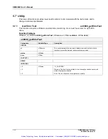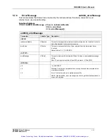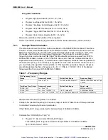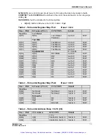
DBS9900 User’s Manual
6-6
DBS9900 Registers
82-28993 Revision 01
Table 4 - STATUS REGISTER - READ ONLY (0x04)
BIT
Name
SET means:
Cleared means:
D0
SOFT RESET
Resets DBS9900 registers
Enables access to DBS9900
D1
SYSFL INHIB
Prevents SYSFAIL assertion
Enables SYSFAIL assertion
D2
PASSED
DC POWER OK
DC POWER FAIL
D3
READY
Self Test is complete
Self Test is in progress
D4
Not Used
Not Used
D5
MOD A INST
Module A is present
Module A is not installed
D6
MOD B INST
Module B is present
Module B is not installed
D7
Not Used
Not Used
D8
MOD A DONE
Module A is done
Module A is busy
D9
MOD B DONE
Module B is done
Module B is busy
D10
Not Used
Not Used
D11
MOD A SPARE
Module A spare
Module A spare
D12
MOD B SPARE
Module B spare
Module B spare
D13
Not Used
Not Used
D14
MODID*
Device not selected
Device selected
D15
A24/A32 ACTIVE
DBS9900 memory access enabled
DBS9900 memory access disabled
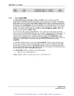
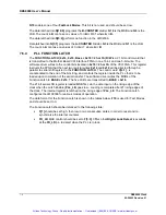
6.5 Memory Offset Register
The 16-bit Memory Offset Register (0x06) defines the base address of the DBS9900’s A24 or
A32 operational registers. The
m
+1 most significant bits of the offset register are the values of
the
m
+1 most significant bits of the A24 or A32 register addresses.
M
is the value of the
required
memory
field of the device type register (0x02).
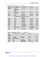
Table 5- Offset Register Bit assignments in A24 and A32 Mode (0x06) R/W
JP1
MODE D:
15
14
13
12
11
10
9
8
7
6
5
4
3
2
1
0
Pins 2&3 A24
A:
23
22
21
20
19
18
17
16
NA NA
NA
NA
NA
NA
NA
NA
Pins 1&2 A32
A:
31
30
29
28
27
26
25
24
23
22
21
20
19
18
17
16
Artisan Technology Group - Quality Instrumentation ... Guaranteed | (888) 88-SOURCE | www.artisantg.com


