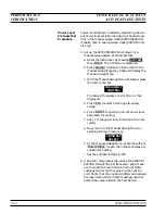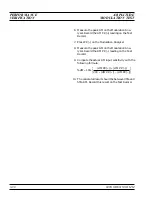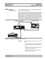
5. On the PN9000, connect the
Fc. 100 MHz OUT-
PUT
of the Crystal Oscillator module to the
2nd
LO INPUT
of the Phase Detector module.
6. On the PN9000, connect the
TUNE VOLTAGE
OUTPUT
of the Lock Control module to the
Fc.
TUNE INPUT
of the Crystal Oscillator module.
Test
Procedure
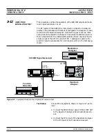
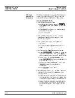
The following procedure lets you measure the RF
output single sideband phase noise levels to verify
that they meet specifications.
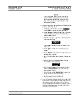
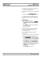
1. Set the 690XXB/691XXB (DUT) GPIB address as
follows:
a. Press
SYSTEM
, then
Config
. The System
Configuration Menu is displayed.
b. Press
GPIB
to display the Configure GPIB
Menu.
c. Press
GPIB Address
to change the current
address of the 690XXB/691XXB (DUT).
d. Enter a new address using the cursor control
key or the data entry keypad and the termina-
tor key
HZ
ns
ADRS
The new address will appear on the display.
The entry must be between 1 and 30 to be
valid.
2. Set the 69XXXB (LO) GPIB address by following
the procedure in step 1. The GPIB address set
must be different from the one set for the
690XXB/691XXB (DUT) in step 1.
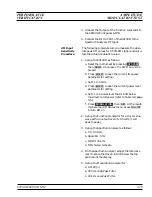
3. On the PN9000, set the frequencies as follows:
a. Select the Measure/Graph menu:
(1) Set Log. Fmin = 10 Hz
(2) Set Log. Fmax = 1 MHz
(3) Set Level max = –30 dB
(4) Set Level min = –140 dB
b. Select Status/Average menu:
(1) Set Average = On
(2) Set 10/100Hz = 40
690XXB/691XXB MM
3-21
PERFORMANCE
SINGLE SIDEBAND
VERIFICATION
PHASE NOISE TEST
Summary of Contents for 680 C Series
Page 4: ......
Page 5: ......
Page 13: ...Figure 1 1 Typical Series 690XXB 691XXB Synthesized CW Signal Generator Model 69187B Shown ...
Page 61: ......
Page 97: ......
Page 205: ......
Page 207: ......
Page 221: ......
Page 225: ......
Page 241: ......
Page 259: ......
Page 275: ......
Page 285: ......
Page 289: ......
Page 299: ......
Page 303: ......
Page 315: ......


