EK76
EK76U Rev A
5
BEFORE YOU GET STARTED
• All Apex Microtechnology amplifiers should be handled using proper ESD precautions.
• Always use the heat sink included in this kit.
• Always use adequate power supply bypassing.
• Do not change the connections while the circuit is powered.
• Initially set all power supplies to the minimum operations levels allowed in the device data sheet.
• Check for oscillations.
• Please refer to Application Note, AN01 for general operating conditions.
ASSEMBLY INSTRUCTIONS
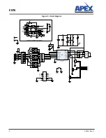
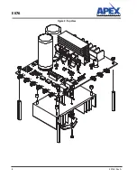
During the assembly, please refer to the circuit schematics, assembly drawings, and the data sheet of the
part being used on the evaluation kit.
1. Note that each side of the EVAL94 circuit board is identified as either the Component side or the DUT
(Device Under Test) side. The component side has the designators printed on that side.
2. First, insert the 16 pin receptacles from the DUT side, into the DUT position. These will be a tight fit, so a
flat piece of metal is recommended as a finger-shield to fully engage the receptacles with the plated
through-holes. This tight fit is meant to keep perpendicularity between the PCB and the pin direction.
Ensure the hexagonal portions go completely through the holes, and the circular flange rests on the DUT
side of the PCB. Solder the pin receptacles from the Component side.
3. Solder the surface-mount capacitors CBP1, CBP2, and CBP3 on the Component side.
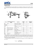
4. If current-sense offset or gain adjustment is required, install the optional components U2 and surrounding
resistors/capacitors. These components are not included, as this is only necessary in unique applications
where current sense must be tightly managed. See "Current Sense" section below.
5. Install the smaller components, including R4-8, D1-6, LED1, and P2. Note that R6 includes a socket to eas
-
ily swap between high-impedance inputs (R6 not installed) and 50-Ohm terminated inputs (R6 installed).
Each element of this resistor can dissipate up to 200mW. Match the direction of R6 with the PCB designa
-
tor when installing. Also match all diode orientations with their respective designators.
6. Use a piece of heavy wire (16 to 14 AWG, 1.3 to 1.8 mm) to short J1. This should be the only connection
between digital ground (DGND) and power ground (PGND).
7. Install P3, P4, and P5 BNC connectors for output sense with an oscilloscope. This is best done by soldering
the center pin first to anchor the component in place, then soldering the 4 external lugs.
8. Install R1, R2, and R3. Their heights must be set by the widened portion of the pins resting on the Compo
-
nent side of the PCB. This will place the plastic package 4mm above the PCB.
9. Apply a thin layer of thermal grease (not included) the backside of R1, R2, and R3. Place the CSR-HS
(CR101-75AE; the smaller of the two included heatsinks) behind these resistors, with the mounting lugs
engaging the PCB holes. Solder these mounting lugs while keeping the heatsink perpendicular to the
board.
10. From either side, slide the cam clips (CLA-TO-21E) into the hooked slot of the CSR-HS. The tabs should be
pointed at a 45° angle down and away from the heatsink. Once the clip is in front of a resistor, flip the tab
all the way up to apply pressure to each resistor.
11. Install P1, P15, and P16.
12. Install electrolytic bypass capacitors CBP4 and CBP5, ensuring that the orientation matches the circuit
schematic drawing.
13. P6 through P14 have edge-connector pads. These pads are designed for edge-mount SMA connectors (not
included). If SMA connection is not desired, leave these pads unpopulated. Otherwise, use recommended
part number CON-SMA-EDGE-S (or similar) and solder these to the board.

