Rev B
7
2. THEORY OF OPERATION
2.1 DESIGN OF THE AMPLIFIER
The Model 500T8G18 TWT amplifier consists of two packages, the supertube and the power supply/control
module. The power supply/control module, in turn, consists of three subsystems. Two of these subsystems,
the microwave components and the TWT power supply, are discussed in sections 2.2 and 2.3, respectively.
The third subsystem is the microprocessor control system. This consists of a number of subassemblies. See
the build tree in section 5.1 for further information about how the parts lists are structured.
The heart of the microprocessor control system is the control head assembly (A22933-300), which consists of
the CPU board (A25450-000) and the data link board (A22488-001). The microprocessor control system
supervises the power supply, provides metering display, processes operator front panel inputs, and enables
communication with a host computer over the IEEE-488 interface. Communication from the front panel is
through the HPA display board (A22700-900).
The control head is provided with its own power supply and, other than thru the IEEE-488 interface bus, is
electrically isolated from the amplifier. Communication with the amplifier is via fiberoptic links to the HPA
interface assembly (A25444-000).
2.2 DESCRIPTION OF THE RF CIRCUIT
The TWTA consists of two stages of RF amplification: a solid state preamp assembly with adjustable gain
(E01415-000) and the dual traveling-wave tubes that are power combined in the RF chassis(E08114-001).
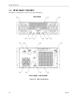
The type N RF input connector is located on the rear panel of the supertube module. The RF input is fed to
the input connector on the solid state preamp. The solid state preamp's output drives the RF input of the TWT
module. The RF output of the TWT is a type WRD-750 waveguide flange on the rear panel of the tube
assembly. A dual directional coupler is built into the tube assembly. The forward output is split off by a -10
dB coupler to provide a forward sample on the rear panel of the supertube. The through output of this coupler
is attenuated by a pad and detected by a zero-bias schottky RF detector. The output of the detector is buffered
by an operational amplifier for noise reduction. The buffered signal is sent to the power supply/control
module and is used for internal forward power metering.
The reflected RF signal is likewise detected and buffered and sent to the power supply/control module. The
detected signal is used for VSWR protection by the power supply logic board, for VSWR measurement in the
leveling loop, and for reflected power measurement on the HPA interface board.
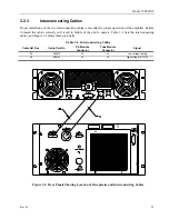
CAUTION:
There are two cables between the power supply/control module and the
supertube assembly. See section 3.2.3, Interconnecting Cables, for
instructions for interconnecting the two modules.
Amplifier gain is determined by the solid state preamp (SSA), which has a voltage-controlled variable gain
stage. The control head determines the output of a digital-to-analog converter (DAC) on the HPA interface
board. The output of the DAC controls the SSA gain. The emergency bypass board (A24830-001) is mounted
behind the front panel. It is provided with a circuit that increases the attenuation so that reflected power is
limited to a level that can be safely sustained without damage to the amplifier (on the order of 100 watts). In
emergency bypass operation (see section 3.7) the gain control signal is provided locally by means of a
Summary of Contents for 10012342
Page 2: ......
Page 4: ......
Page 8: ......
Page 12: ......
Page 20: ......
Page 44: ...Model 500T8G18 30 Rev B ...
Page 48: ...Model 500T8G18 34 Rev B ...
Page 50: ...Model 500T8G18 36 Rev B ...
Page 56: ...Model 500T8G18 42 Rev B ...
Page 70: ...Model 500T8G18 56 Rev B ...
Page 72: ......

