Model 350S1G6A
36
Rev C
7.
Check the voltages on the feed caps on the A8, A10-A13, A15, A24-A27, A32-A47, A52-A55 quad
amps. Troubleshoot any incorrect voltages.
C2
+25.7 V
±
0.5 V
C1
-5 V
±
0.3 V
C3
logic high (no fault)
4.3.9
Low or No Power Output (RF Test) (Schematic 10047656)
NOTE: The DC Tests specified in Section 4.3.8 should be completed before conducting the RF tests specified
in the following sections.
1.
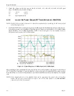
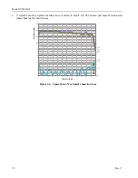
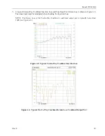
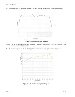
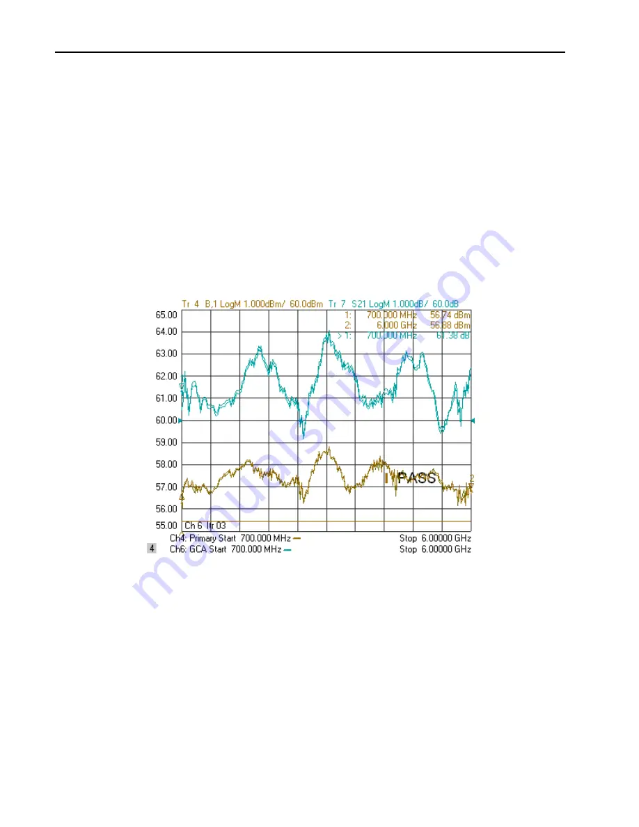
The Model 350S1G6A’s typical gain response at 0 dBm input and -20 dBm input is shown in Figures 4-1.
The actual gain may vary considerably from that shown in Figure 4-1
but should be ≥ 5
5.4 dBm (0 dBm
Input).
should be ≥
59 (-20 dBm Input) dBm.
NOTE: If the overall gain is low, the amplifier chain can
be separated at the input of A3 Two-Way Splitter.
Figure 4-1. Typical Response at 0 dBm Input and -20 dBm Input
Phase matching must be maintained from the input of the A3 Two-Way Splitter to the inputs of both A56 and
A57 Twelve-Way Combiners; if coaxial cables are removed, they must be reinstalled in the same locations
from which they were removed. Replacement coaxial cable assemblies must the same lengths as the original
ones.
NOTE: If the original gain is low, the amplifier chain can be separated at the input to the A3 Two-Way
Splitter and the gain checked from the input to the A3 Two-Way Splitter to the
RF OUTPUT
connector on the unit’s front panel.

