Model 500A250D
Rev A
33
4.3.7
Low or No Power Output (RF Test) (Schematic Diagrams
10045748 and 10039874)
NOTE: The DC Tests specified in Section 4.3.8 should be completed before conducting the RF tests specified
in the following sections.
1.
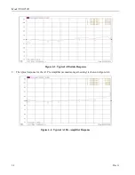
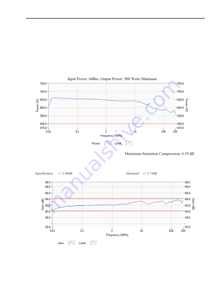
The Model 500A250D’s typical gain response at -20 dBm input and 0 dBm input is shown in Figure 4-1
and Figure 4-2. The actual gain may vary considerably from that shown in Figure 4-1
but should be ≥
57dBm at 0dBm input.
Figure 4-1. Typical Response at -20dBm Input
Figure 4-2. Typical Response at 0 dBm Input
Summary of Contents for 500A250D
Page 2: ......
Page 4: ......
Page 6: ......
Page 18: ......
Page 22: ...Model 500A250D 4 Rev A ...
Page 25: ...Page 3 500A250D 500 watts CW 10kHz 250MHz Graphs ...
Page 26: ...Page 4 500A250D 500 watts CW 10kHz 250MHz Graphs ...
Page 28: ......
Page 46: ...Model 500A250D 24 Rev A ...
Page 58: ......


