background image

B1.18 

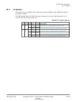
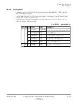
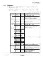
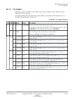
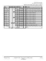
c15 registers

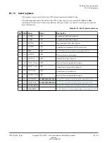
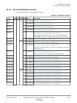
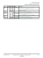
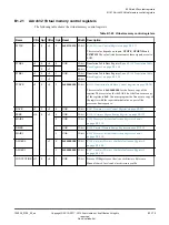
The processor can access different 32-bit wide system registers. Registers where CRn has the value
fifteen are called c15 registers.

The following table shows the 32-bit wide system registers you can access when the processor is in
AArch32 state and the value of CRn is c15.

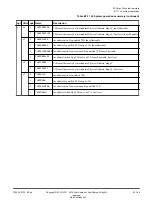
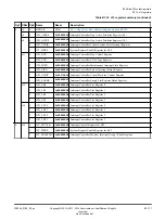
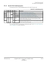
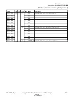
Table B1-17  c15 register summary

Op1 CRm Op2 Name

Reset

Description

1

c0

0

L2ACTLR

0x80000000

B1.91 L2 Auxiliary Control Register

 on page B1-301

This is the reset value for an ACE interface. For an AXI interface the reset value is

0x80000008

. For a CHI interface the reset value is 

0x80004008

.

c3

0

CBAR

-

B1.38 Configuration Base Address Register

 on page B1-200

The reset value depends on the processor configuration.

3

c0

0

CDBGDR0 UNK

Cache Debug Data Register 0, see 

C5.1 About direct access to internal memory

on page C5-608

1

CDBGDR1 UNK

Cache Debug Data Register 1, see 

C5.1 About direct access to internal memory

on page C5-608

2

CDBGDR2 UNK

Cache Debug Data Register 2, see 

C5.1 About direct access to internal memory

on page C5-608

3

CDBGDR3 UNK

Cache Debug Data Register 3, see 

C5.1 About direct access to internal memory

on page C5-608

c2

0

CDBGDCT UNK

Cache Debug Data Cache Tag Read Operation Register, see 

C5.1 About direct

access to internal memory

 on page C5-608

1

CDBGICT

UNK

Cache Debug Instruction Cache Tag Read Operation Register, see 

C5.1 About direct

access to internal memory

 on page C5-608

c4

0

CDBGDCD UNK

Cache Debug Cache Debug Data Cache Data Read Operation Register, see

C5.1 About direct access to internal memory

 on page C5-608

1

CDBGICD

UNK

Cache Debug Instruction Cache Data Read Operation Register, see 

C5.1 About

direct access to internal memory

 on page C5-608

2

CDBGTD

UNK

Cache Debug TLB Data Read Operation Register, see 

C5.1 About direct access to

internal memory

 on page C5-608

B1 AArch32 system registers

B1.18 c15 registers

100236_0100_00_en

Copyright © 2015–2017, 2019 Arm Limited or its affiliates. All rights

reserved.

B1-174

Non-Confidential

Summary of Contents for Cortex-A35

Page 1: ...Arm Cortex A35 Processor Revision r1p0 Technical Reference Manual Copyright 2015 2017 2019 Arm Limited or its affiliates All rights reserved 100236_0100_00_en ...

Page 2: ...LIABLE FOR ANY DAMAGES INCLUDING WITHOUT LIMITATION ANY DIRECT INDIRECT SPECIAL INCIDENTAL PUNITIVE OR CONSEQUENTIAL DAMAGES HOWEVER CAUSED AND REGARDLESS OF THE THEORY OF LIABILITY ARISING OUT OF ANY USE OF THIS DOCUMENT EVEN IF ARM HAS BEEN ADVISED OF THE POSSIBILITY OF SUCH DAMAGES This document consists solely of commercial items You shall be responsible for ensuring that any use duplication o...

Page 3: ...the agreement entered into by Arm and the party that Arm delivered this document to Unrestricted Access is an Arm internal classification Product Status The information in this document is Final that is for a developed product Web Address http www arm com Arm Cortex A35 Processor 100236_0100_00_en Copyright 2015 2017 2019 Arm Limited or its affiliates All rights reserved 3 Non Confidential ...

Page 4: ......

Page 5: ...tion options A1 32 A1 4 Supported standards and specifications A1 34 A1 5 Test features A1 35 A1 6 Design tasks A1 36 A1 7 Product revisions A1 37 Chapter A2 Technical Overview A2 1 Components A2 40 A2 2 Interfaces A2 44 A2 3 About system control A2 46 A2 4 About the Generic Timer A2 47 A2 5 About the memory model A2 48 100236_0100_00_en Copyright 2015 2017 2019 Arm Limited or its affiliates All r...

Page 6: ...YWFI 3 0 and STANDBYWFIL2 signals A4 75 A4 17 Q channel A4 76 Chapter A5 Cache Behavior and Cache Protection A5 1 Cached memory types A5 78 A5 2 Coherency between data caches with the MOESI protocol A5 79 A5 3 Cache misses unexpected cache hits and speculative fetches A5 80 A5 4 Disabling a cache A5 81 A5 5 Invalidating or cleaning a cache A5 82 A5 6 About read allocate mode A5 83 A5 7 About cache...

Page 7: ...CHI transactions A10 131 Chapter A11 ACP Slave Interface A11 1 About the ACP A11 136 A11 2 Transfer size support A11 137 A11 3 ACP performance A11 138 A11 4 ACP user signals A11 139 Chapter A12 GIC CPU Interface A12 1 Bypassing the GIC CPU Interface A12 142 A12 2 Memory map for the GIC CPU interface A12 143 Part B Register Descriptions Chapter B1 AArch32 system registers B1 1 AArch32 register summ...

Page 8: ...Control Register B1 206 B1 42 CPU Auxiliary Control Register B1 208 B1 43 CPU Extended Control Register B1 212 B1 44 CPU Memory Error Syndrome Register B1 214 B1 45 Cache Size Selection Register B1 217 B1 46 Cache Type Register B1 219 B1 47 Domain Access Control Register B1 221 B1 48 Data Fault Address Register B1 222 B1 49 Data Fault Status Register B1 223 B1 50 DFSR with Short descriptor transla...

Page 9: ...t B1 297 B1 90 Interrupt Status Register B1 299 B1 91 L2 Auxiliary Control Register B1 301 B1 92 L2 Control Register B1 303 B1 93 L2 Extended Control Register B1 305 B1 94 L2 Memory Error Syndrome Register B1 307 B1 95 Memory Attribute Indirection Registers 0 and 1 B1 310 B1 96 Main ID Register B1 313 B1 97 Multiprocessor Affinity Register B1 315 B1 98 Non Secure Access Control Register B1 317 B1 ...

Page 10: ... 17 AArch64 Thread registers B2 383 B2 18 AArch64 Implementation defined registers B2 384 B2 19 Auxiliary Control Register EL1 B2 386 B2 20 Auxiliary Control Register EL2 B2 387 B2 21 Auxiliary Control Register EL3 B2 389 B2 22 Auxiliary Fault Status Register 0 EL1 EL2 and EL3 B2 391 B2 23 Auxiliary Fault Status Register 1 EL1 EL2 and EL3 B2 392 B2 24 Auxiliary ID Register EL1 B2 393 B2 25 Auxilia...

Page 11: ... Model Feature Register 2 EL1 B2 471 B2 66 AArch32 Memory Model Feature Register 3 EL1 B2 473 B2 67 AArch32 Processor Feature Register 0 EL1 B2 475 B2 68 AArch32 Processor Feature Register 1 EL1 B2 477 B2 69 Instruction Fault Status Register EL2 B2 479 B2 70 IFSR32_EL2 with Short descriptor translation table format B2 480 B2 71 IFSR32_EL2 with Long descriptor translation table format B2 482 B2 72 ...

Page 12: ...tual interface control register summary B3 563 B3 5 VGIC Type Register B3 564 B3 6 Virtual CPU interface register summary B3 565 B3 7 VM Active Priority Register B3 566 B3 8 VM CPU Interface Identification Register B3 567 Chapter B4 Generic Timer registers B4 1 Generic Timer register summary B4 570 B4 2 AArch32 Generic Timer register summary B4 571 B4 3 AArch64 Generic Timer register summary B4 57...

Page 13: ...chpoint Control Registers EL1 C7 639 Chapter C8 Memory mapped debug registers C8 1 Memory mapped debug register summary C8 644 C8 2 External Debug Reserve Control Register C8 648 C8 3 External Debug Integration Mode Control Register C8 650 C8 4 External Debug Device ID Register 0 C8 651 C8 5 External Debug Device ID Register 1 C8 652 C8 6 External Debug Processor Feature Register C8 653 C8 7 Exter...

Page 14: ...ister EL0 C10 704 C10 7 Performance Monitors Common Event Identification Register 0 EL0 C10 707 C10 8 Performance Monitors Common Event Identification Register 1 EL0 C10 711 C10 9 Memory mapped PMU register summary C10 714 C10 10 Performance Monitors Configuration Register C10 717 C10 11 Performance Monitors Peripheral Identification Registers C10 719 C10 12 Performance Monitors Peripheral Identif...

Page 15: ... Implementation Specific Register 0 C11 772 C11 32 ID Register 0 C11 773 C11 33 ID Register 1 C11 775 C11 34 ID Register 2 C11 776 C11 35 ID Register 3 C11 778 C11 36 ID Register 4 C11 780 C11 37 ID Register 5 C11 782 C11 38 Resource Selection Control Registers 2 16 C11 784 C11 39 Single Shot Comparator Control Register 0 C11 785 C11 40 Single Shot Comparator Status Register 0 C11 786 C11 41 OS Lo...

Page 16: ...rigger register summary C12 826 C12 2 External register access permissions to the CTI registers C12 828 C12 3 CTI Device Identification Register C12 829 C12 4 CTI Integration Mode Control Register C12 831 C12 5 CTI Peripheral Identification Registers C12 832 C12 6 CTI Peripheral Identification Register 0 C12 833 C12 7 CTI Peripheral Identification Register 1 C12 834 C12 8 CTI Peripheral Identifica...

Page 17: ... signals Appx A 876 A 19 CTI interface signals Appx A 877 A 20 DFT interface signals Appx A 878 A 21 MBIST interface signals Appx A 879 Appendix B AArch32 UNPREDICTABLE Behaviors B 1 Use of R15 by Instruction Appx B 882 B 2 UNPREDICTABLE instructions within an IT Block Appx B 883 B 3 Load Store accesses crossing page boundaries Appx B 884 B 4 Armv8 Debug UNPREDICTABLE behaviors Appx B 885 B 5 Othe...

Page 18: ......

Page 19: ...Arm Cortex A35 Processor Technical Reference Manual It contains the following About this book on page 20 Feedback on page 25 100236_0100_00_en Copyright 2015 2017 2019 Arm Limited or its affiliates All rights reserved 19 Non Confidential ...

Page 20: ...and Input Synchronization This chapter describes the clocks of the Cortex A35 processor It also describes the reset options Chapter A4 Power Management This chapter describes the power domains and the power modes in the Cortex A35 processor Chapter A5 Cache Behavior and Cache Protection This chapter describes the CPU and SCU cache protection features of the Cortex A35 processor Chapter A6 L1 Memor...

Page 21: ...registers in the AArch32 execution state and shows examples of how to use them Chapter C7 AArch64 debug registers This chapter describes the debug registers in the AArch64 execution state and shows examples of how to use them Chapter C8 Memory mapped debug registers This chapter describes the debug memory mapped registers and shows examples of how to use them Chapter C9 ROM table This chapter desc...

Page 22: ...option name monospace italic Denotes arguments to monospace text where the argument is to be replaced by a specific value monospace bold Denotes language keywords when used outside example code and Encloses replaceable terms for assembler syntax where they appear in code or code fragments For example MRC p15 0 Rd CRn CRm Opcode_2 SMALL CAPITALS Used in body text for a few terms that have specific ...

Page 23: ...er Interface Specification Q Channel and P Channel Interfaces IHI 0068 Arm Architecture Reference Manual Armv8 for Armv8 A architecture profile DDI 0487 Arm Generic Interrupt Controller Architecture Specification IHI 0069 Arm Embedded Trace Macrocell Architecture Specification ETMv4 IHI 0064 Arm CoreSight Architecture Specification IHI 0029 Arm Cortex A Series Programmer s Guide for Armv8 A DEN 00...

Page 24: ...ic Note Arm floating point terminology is largely based on the earlier ANSI IEEE Std 754 1985 issue of the standard See the Arm Architecture Reference Manual Armv8 for Armv8 A architecture profile for more information Preface Additional reading 100236_0100_00_en Copyright 2015 2017 2019 Arm Limited or its affiliates All rights reserved 24 Non Confidential ...

Page 25: ... com Give The title Arm Cortex A35 Processor Technical Reference Manual The number 100236_0100_00_en If applicable the page number s to which your comments refer A concise explanation of your comments Arm also welcomes general suggestions for additions and improvements Note Arm tests the PDF only in Adobe Acrobat and Acrobat Reader and cannot guarantee the quality of the represented document when ...

Page 26: ......

Page 27: ...Part A Functional Description ...

Page 28: ......

Page 29: ...ocessor on page A1 30 A1 2 Features on page A1 31 A1 3 Implementation options on page A1 32 A1 4 Supported standards and specifications on page A1 34 A1 5 Test features on page A1 35 A1 6 Design tasks on page A1 36 A1 7 Product revisions on page A1 37 100236_0100_00_en Copyright 2015 2017 2019 Arm Limited or its affiliates All rights reserved A1 29 Non Confidential ...

Page 30: ... that allows for I O coherent operations with an external master for example a DMA engine The following figure shows an example configuration with four cores an L2 cache and a CHI system bus interface CHI DFT Q channel MBIST Processor SCU Debug L2 cache Optional Power management Test AXI ACP Core 0 Core 1 Core 2 Core 3 CoreSight infrastructure Interrupt interface Figure A1 1 Example processor conf...

Page 31: ...al data engine that implements the Advanced SIMD and floating point architecture support Optional Cryptographic Extension This architectural extension is only available if the data engine is present Armv8 debug logic Performance Monitoring Unit PMU Optional Embedded Trace Macrocell ETM that supports instruction trace only Optional Generic Interrupt Controller GIC CPU interface to connect to an ext...

Page 32: ... implemented without SCU L2 cache protection Also protects the L1 duplicate tags in the SCU GIC CPU interface Included Not included ETM Included Not included Advanced SIMD and floating point support Included Not included Advanced SIMD and floating point support is configured on a per core basis Cryptographic Extension Included Not included If the Cryptographic Extension is included then it is incl...

Page 33: ... SCU L2 If the processor does not include an L2 cache it cannot implement the ACP Debug memory map v8 debug memory map v7 debug memory map Related information A2 2 Interfaces on page A2 44 A5 5 Invalidating or cleaning a cache on page A5 82 A6 1 About the L1 memory system on page A6 90 A7 1 About the L2 memory system on page A7 98 A5 7 About cache protection on page A5 84 Chapter A12 GIC CPU Inter...

Page 34: ... the Cryptographic Extension without the Advanced SIMD and floating point support Interconnect AMBA 4 AXI AMBA 4 ACE AMBA 5 CHI You can also connect the processor to an AMBA 3 AXI interconnect Generic Interrupt Controller v4 Generic Timer Armv8 A PMU v3 Debug Armv8 CoreSight v2 Embedded Trace Macrocell ETMv4 Related information Arm Architecture Reference Manual Armv8 for Armv8 A architecture profi...

Page 35: ... to test the processor and its memory arrays Related information A 20 DFT interface signals on page Appx A 878 A 21 MBIST interface signals on page Appx A 879 A1 Introduction A1 5 Test features 100236_0100_00_en Copyright 2015 2017 2019 Arm Limited or its affiliates All rights reserved A1 35 Non Confidential ...

Page 36: ...the processor and tests the application software The operation of the final device depends on the following Build configuration The implementer chooses the options that affect how the RTL source files are pre processed These options usually include or exclude logic that affects one or more of the area maximum frequency and features of the resulting macrocell Configuration inputs The integrator con...

Page 37: ...here are no functional changes in this release r0p2 There are no functional changes in this release r1p0 New CP15SDISABLE2 signal and new asymmetric floating point NEON feature A1 Introduction A1 7 Product revisions 100236_0100_00_en Copyright 2015 2017 2019 Arm Limited or its affiliates All rights reserved A1 37 Non Confidential ...

Page 38: ...A1 Introduction A1 7 Product revisions 100236_0100_00_en Copyright 2015 2017 2019 Arm Limited or its affiliates All rights reserved A1 38 Non Confidential ...

Page 39: ...lowing sections A2 1 Components on page A2 40 A2 2 Interfaces on page A2 44 A2 3 About system control on page A2 46 A2 4 About the Generic Timer on page A2 47 A2 5 About the memory model on page A2 48 100236_0100_00_en Copyright 2015 2017 2019 Arm Limited or its affiliates All rights reserved A2 39 Non Confidential ...

Page 40: ... protection and the Cryptographic Extension The following figure shows a top level functional diagram of the Cortex A35 processor Core 1 governor block Core 3 Core 2 ETM Core 0 GIC CPU interface CTI SCU L2 ACP Processor Timer CTM APB L2 cache Core 1 Governor Core 0 governor block IFU Micro TLB SCU Core 2 governor block Core 3 governor block ETM DPU PMU Micro TLB Neon L1 memory system L1 ICache L1 ...

Page 41: ...Note The Advanced SIMD architecture its associated implementations and supporting software are also referred to as NEON technology Cryptographic Extension The optional Cortex A35 processor Cryptographic Extension supports the Armv8 Cryptographic Extensions It can be configured at implementation time and applies to all cores that implement Advanced SIMD and floating point support The Cryptographic ...

Page 42: ...he STB is also used to queue maintenance operations before they are broadcast to other cores in the processor BIU The BIU contains the SCU interface and buffers to decouple the interface from the L1 Data cache and STB The BIU and the SCU always operate at the processor frequency Governor The governor block outside the core includes all functions that must remain operating while a core is in retent...

Page 43: ...ocate data in the L2 cache RAMs Debug and trace components Cross trigger The Cross Trigger Matrix CTM combines the CoreSight Cross Trigger Interface CTI channel signals from all the cores so that a single cross trigger channel interface is presented in the Cortex A35 processor This module can combine up to four internal channel interfaces corresponding to each core along with one external channel ...

Page 44: ...r masters and allows other masters to allocate data into the L2 cache It allows an external master to make coherent requests to shared memory but it does not support cache maintenance coherency barrier or DVM transactions Debug APB Allows access to debug registers and resources for example to set watchpoints and breakpoints Cross trigger CTI This external interface is connected to the CoreSight CT...

Page 45: ...n page C4 604 Arm AMBA AXI and ACE Protocol Specification AXI3 AXI4 and AXI4 Lite and ACE and ACE Lite Arm AMBA 5 CHI Protocol Specification Arm CoreSight Architure Specification A2 Technical Overview A2 2 Interfaces 100236_0100_00_en Copyright 2015 2017 2019 Arm Limited or its affiliates All rights reserved A2 45 Non Confidential ...

Page 46: ...m Control Register SCTLR Translation Table Base Register 1 TTBR1 Translation Table Base Control Register TTBCR Domain Access Control Register DACR Primary Region Remap Register PRRR Normal Memory Remap Register NMRR Memory Attribute Indirection Register 0 MAIR0 Memory Attribute Indirection Register 1 MAIR1 Vector Base Address Register VBAR Monitor Vector Base Address Register MVBAR Reset Managemen...

Page 47: ...gistered inside the processor and then used as a clock enable for CNTVALUEB 63 0 This allows a multicycle path to be applied to the CNTVALUEB 63 0 The following figure shows the interface Processor Clock gate CNTCLKEN register Architectural counter registers CNTVALUEB 63 0 CNTCLKEN Figure A2 3 Generic Timer interface The value on CNTVALUEB 63 0 is required to be stable whenever the internally regi...

Page 48: ...he second stored word The processor can store words in memory in big endian or little endian format Instructions are always little endian Related information ARM Architecture Reference Manual ARMv8 for ARMv8 A architecture profile A2 Technical Overview A2 5 About the memory model 100236_0100_00_en Copyright 2015 2017 2019 Arm Limited or its affiliates All rights reserved A2 48 Non Confidential ...

Page 49: ...tex A35 processor It also describes the reset options It contains the following sections A3 1 Clocks on page A3 50 A3 2 Input synchronization on page A3 51 A3 3 Resets on page A3 52 100236_0100_00_en Copyright 2015 2017 2019 Arm Limited or its affiliates All rights reserved A3 49 Non Confidential ...

Page 50: ...LKIN The Cortex A35 processor has the following clock enable signals PCLKENDBG ACLKENM ACLKENS SCLKEN ATCLKEN CNTCLKEN For more information see the Arm Cortex A35 Processor Integration Manual A3 Clocks Resets and Input Synchronization A3 1 Clocks 100236_0100_00_en Copyright 2015 2017 2019 Arm Limited or its affiliates All rights reserved A3 50 Non Confidential ...

Page 51: ...IRQACK DBGEN EDBGRQ EVENTI L2FLUSHREQ L2QREQn NEONQREQn NIDEN SPIDEN SPNIDEN Input signals that the Cortex A35 processor synchronizes under certain conditions CTICHIN The synchronized CTICHIN input signals are used only if the CISBYPASS input signal is deasserted LOW If the CISBYPASS signal is asserted HIGH the CTICHIN synchronizers are not used and the SoC must present the CTICHIN synchronously t...

Page 52: ... and exit from MBIST mode Reset synchronization logic inside the processor ensures that reset deassertion is synchronous for all resettable registers The processor clock is not required for reset assertion but it must be present for reset deassertion to ensure reset synchronization In general the reset time only requires three processor clock cycles Note The application of a retention state can af...

Page 53: ...dividual core cold reset with debug active nCPUPORESET CN 0 nCORERESET CN 0 nPRESETDBG nL2RESET nMBISTRESET n 0 n X 1 1 1 Individual core is held in reset so that the core can be powered up This enables external debug over power down for the core that is held in reset nCORERESET can be asserted but is not required Individual core warm reset with trace and debug active nCPUPORESET CN 0 nCORERESET C...

Page 54: ...rect sequence before applying Warm reset to that core For individual processor Warm reset You must apply steps 1 to 6 in the core powerdown sequence see A4 6 Powering down an individual core on page A4 65 and wait until STANDBYWFI is asserted indicating that the core is idle before asserting nCORERESET for that core nCORERESET for that core must assert for at least 3 CLK cycles nL2RESET must not a...

Page 55: ...bugger might also request a Warm reset of the core by asserting DBGRSTREQ See the Arm Architecture Reference Manual Armv8 for Armv8 A architecture profile for information about the recommended code sequence to use to request a Warm reset You must apply steps 1 on page A4 65 to 6 on page A4 65 in the core powerdown sequence in A4 6 Powering down an individual core on page A4 65 and wait until STAND...

Page 56: ...A3 Clocks Resets and Input Synchronization A3 3 Resets 100236_0100_00_en Copyright 2015 2017 2019 Arm Limited or its affiliates All rights reserved A3 56 Non Confidential ...

Page 57: ...ut system driven L2 flush on page A4 67 A4 9 Powering up the processor without system driven L2 flush on page A4 68 A4 10 Powering down the processor with system driven L2 flush on page A4 69 A4 11 Powering up the processor with system driven L2 flush on page A4 70 A4 12 Entering Dormant mode on page A4 71 A4 13 Exiting Dormant mode on page A4 72 A4 14 Event communication using WFE or SEV on page ...

Page 58: ...floating point support the L1 cache and TLB RAMs and the debug registers that are described as being in the processor domain n is 0 1 2 or 3 It represents core 0 core 1 core 2 or core 3 If a core is not present the corresponding power domain is not present PDCPUADVSIMD n Represents the Advanced SIMD and floating point block of core n n is 0 1 2 or 3 It represents core 0 core 1 core 2 or core 3 If ...

Page 59: ...d down domains However only some powered up and powered down domain combinations are valid and supported Table A4 2 Power state description Power state Description Off Block is power gated Ret Logic or RAM retention power only On Block is active The following tables show the supported power domain states for the processor Caution States that are not shown in the tables are unsupported and must not...

Page 60: ... supported power domain states for individual cores The power domain state in each core is independent of all other cores Table A4 4 Supported core power states Power domains Description PDCPU PDADVSIMD Off Off Core off On On Core on Advanced SIMD and floating point on On Ret AdvSIMD retention Advanced SIMD and floating point in retention Ret Ret Core retention Core logic and Advanced SIMD and flo...

Page 61: ...uction L2 standby mode When all the cores are in standby mode and the L2 memory system is idle Individual core shutdown mode The PDCPU power domain for an individual core is shut down and the state held in this domain is lost Cluster shutdown mode The PDMERCURY PDL2 and all PDCPU power domains are shut down and the state held in these domains is lost Dormant mode optional All the cores and L2 cont...

Page 62: ...FI low power state the clocks in the core are temporarily enabled without causing the core to exit WFI low power state when any of the following events are detected A snoop request that must be serviced by the core L1 Data cache A cache or TLB maintenance operation that must be serviced by the core L1 Instruction cache data cache or TLB An APB access to the debug or trace registers residing in the...

Page 63: ...om WFE low power state occurs when the core detects a reset the assertion of the EVENTI input signal or one of the WFE wake up events as described in the Arm Architecture Reference Manual Armv8 for Armv8 A architecture profile On entry into WFE low power state STANDBYWFE for that core is asserted Assertion of STANDBYWFE guarantees that the core is in idle and low power state STANDBYWFE continues t...

Page 64: ...ace the SoC asserts the AINACTS input pin to idle the ACP interface It indicates that the SoC sends no more transactions on the ACP interface When the L2 memory system completes the outstanding transactions for AXI ACE or CHI interfaces it can then enter the L2 WFI low power state On entry into L2 WFI low power state STANDBYWFIL2 is asserted Assertion of STANDBYWFIL2 guarantees that the L2 memory ...

Page 65: ...erency with other cores in the cluster by clearing the CPUECTLR SMPEN bit Clearing the SMPEN bit enables the core to be taken out of coherency by preventing the core from receiving cache or TLB maintenance operations broadcast by other cores in the cluster 4 Execute an ISB instruction to ensure that all of the register changes from the previous steps have been committed 5 Execute a DSB SY instruct...

Page 66: ...CPUPORESET and DBGPWRDUP LOW 3 Release the core output clamps 4 Deassert resets 5 Set the CPUECTLR SMPEN bit to 1 to enable snooping into the core 6 Assert DBGPWRDUP HIGH to allow external debug access to the core 7 If required use software to restore the state of the core as it was before powerdown A4 Power Management A4 7 Powering up an individual core 100236_0100_00_en Copyright 2015 2017 2019 ...

Page 67: ...to the interface does not send new transactions then assert AINACTS 4 Clean and invalidate all data from the L2 Data cache 5 Follow steps 3 on page A4 65 to 10 on page A4 65 in A4 6 Powering down an individual core on page A4 65 6 In an ACE configuration assert ACINACTM or in a CHI configuration assert SINACT Then wait until the STANDBYWFIL2 output is asserted to indicate that the L2 memory system...

Page 68: ...ert nCPUPORESET LOW 2 Assert nL2RESET LOW and hold L2RSTDISABLE LOW 3 Apply power to the PDMERCURY and PDL2 domains while keeping the signals described in steps 1 on page A4 68 and 2 on page A4 68 LOW 4 Release the cluster output clamps 5 Continue a normal cold reset sequence A4 Power Management A4 9 Powering up the processor without system driven L2 flush 100236_0100_00_en Copyright 2015 2017 201...

Page 69: ...sh is occurring 3 Assert L2FLUSHREQ HIGH 4 Hold L2FLUSHREQ HIGH until L2FLUSHDONE is asserted 5 Deassert L2FLUSHREQ 6 In an ACE configuration assert ACINACTM or in a CHI configuration assert SINACT Then wait until the STANDBYWFIL2 output is asserted to indicate that the L2 memory system is idle All Cortex A35 processor implementations contain an L2 memory system including implementations without a...

Page 70: ...DISABLE LOW 3 Apply power to the PDMERCURY and PDL2 domains while keeping the signals described in steps 1 on page A4 70 and 2 on page A4 70 LOW 4 Release the cluster output clamps 5 Continue a normal cold reset sequence A4 Power Management A4 11 Powering up the processor with system driven L2 flush 100236_0100_00_en Copyright 2015 2017 2019 Arm Limited or its affiliates All rights reserved A4 70 ...

Page 71: ...tem registers are saved All debug related state is saved 5 Execute an ISB instruction to ensure that all of the register changes from the previous steps have been committed 6 Execute a DSB instruction to ensure that all cache TLB and branch predictor maintenance operations issued by any core in the cluster before the SMPEN bit was cleared have completed In addition this ensures that all state savi...

Page 72: ...d reset sequence You must apply resets to the cores and the L2 memory system logic until power is restored During this reset sequence L2RSTDISABLE must be held HIGH to disable the L2 cache hardware reset mechanism 2 When power has been restored release the L2 cache RAM input clamps 3 Continue a normal cold reset sequence with L2RSTDISABLE held HIGH 4 The architectural state must be restored if req...

Page 73: ...he EVENTI input pin must remain HIGH for at least one CLKIN clock cycle to be visible by the cores The external agent can determine that at least one of the cores in the cluster has executed an SEV instruction by checking the EVENTO pin When SEV is executed by any of the cores in the cluster an event is signaled to all the cores in the device and the EVENTO pin is asserted This pin is asserted HIG...

Page 74: ... controller can be performed using one or both of the A4 16 STANDBYWFI 3 0 and STANDBYWFIL2 signals on page A4 75 A4 17 Q channel on page A4 76 A4 Power Management A4 15 Communication to the Power Management Controller 100236_0100_00_en Copyright 2015 2017 2019 Arm Limited or its affiliates All rights reserved A4 74 Non Confidential ...

Page 75: ...35 processor includes a minimal L2 memory system in configurations without an L2 cache Therefore the power management controller must always wait for assertion of STANDBYWFIL2 before removing power from the Cortex A35 processor This applies to configurations that use the mini SCU and configurations that use the SCU The following figure shows how STANDBYWFI 3 0 and STANDBYWFIL2 correspond to indivi...

Page 76: ...for exit from the quiescent state The associated signaling can contain contributions from other devices in the same power domain Optional device capability to deny a quiescence request Safe asynchronous interfacing across clock domains For more information see the Low Power Interface Specification Arm Q Channel and P Channel Interfaces A4 Power Management A4 17 Q channel 100236_0100_00_en Copyrigh...

Page 77: ...I protocol on page A5 79 A5 3 Cache misses unexpected cache hits and speculative fetches on page A5 80 A5 4 Disabling a cache on page A5 81 A5 5 Invalidating or cleaning a cache on page A5 82 A5 6 About read allocate mode on page A5 83 A5 7 About cache protection on page A5 84 A5 8 Error reporting on page A5 86 A5 9 Error injection on page A5 87 100236_0100_00_en Copyright 2015 2017 2019 Arm Limit...

Page 78: ...Write Back Outer Write Back Data might not be allocated if The data is for a non temporal load The data is for a DC ZVA instruction The transient hint is set The no allocate hint is set The processor is in read allocate mode L2 cache If the L2 cache is present and enabled it can cache the following memory types Normal Inner Write Back Outer Write Back Instruction cache lines are allocated into the...

Page 79: ...ache and is clean Shared SharedClean The line is possibly in more than one cache and is clean Invalid Invalid The line is not in this cache Data coherency is enabled only when the CPUECTLR SMPEN bit is set You must set the SMPEN bit before enabling the data cache If you do not then the cache is not coherent with other cores and data corruption could occur Related information A5 6 About read alloca...

Page 80: ...xecutes an instruction Instruction fetches are therefore speculative A branch or exceptional instruction in the code stream can cause a pipeline flush and discard the fetched instructions Because of the prefetching behavior you must not place read sensitive devices in the same page as code Pages with Device memory type attributes are treated as Non Cacheable Normal Memory when accessed by instruct...

Page 81: ...fetches do not access the L2 unified cache Data cache maintenance operations to the L1 data cache and the L2 unified cache execute normally All load and store instructions to cacheable memory are treated as if they were non cacheable This means that they are not coherent with the caches in this core or the caches in other cores and software must take account of this You cannot disable the L1 data ...

Page 82: ...te DCISW operations in AArch32 and DC ISW instructions in AArch64 perform both a clean and invalidate of the target set way The values of HCR SWIO and HCR_EL2 SWIO have no effect The Armv8 A architecture does not support an operation to invalidate the entire data cache If this function is required in software it must be constructed by iterating over the cache geometry and executing a series of ind...

Page 83: ...they write out to L2 rather than starting a linefill More than the specified number of linefills might be observed on the master interface before the core detects that three full cache lines have been written and switches to read allocate mode The core continues in read allocate mode until it detects either a cacheable write burst to L2 that is not a full cache line or there is a load to the same ...

Page 84: ...he access that caused the error while it corrects the error When the correction is complete the access either continues with the corrected data or is retried If the access is retried it either hits in the cache again with the corrected data or misses in the cache and re fetches the data from a lower level cache or from main memory Table A5 2 Cache protection behavior of each RAM RAM Protection typ...

Page 85: ...itional cycle or two while the correction takes place After correction the processor might evict the line If a correctable ECC error occurs after the first data cache access of a load instruction that takes multiple cycles to complete and if one of the following conditions has taken place A hardware breakpoint watchpoint or vector catch has been set since the first execution that is triggered on r...

Page 86: ...ed until the error is cleared by a write of 0 to the L2 internal asynchronous error bit of the L2ECTLR register Arm recommends that the nINTERRIRQ signal is connected to the interrupt controller so that an interrupt or system error is generated when the signal is asserted When a dirty cache line with an error on the data RAMs is evicted from the processor the write on the master interface still ta...

Page 87: ... Error injection on the L2 data RAMs is enabled by setting the L2ACTLR L2DEIEN bit While this bit is set double bit errors are injected on all writes to the L2 cache data RAMs The L2 data RAMs can be written to because of Explicit stores from one of the cores Instruction fetches or prefetches Evictions from the L1 Data cache ACP accesses Error injection on the L2 tag RAMs is enabled by setting the...

Page 88: ...A5 Cache Behavior and Cache Protection A5 9 Error injection 100236_0100_00_en Copyright 2015 2017 2019 Arm Limited or its affiliates All rights reserved A5 88 Non Confidential ...

Page 89: ...About the L1 memory system on page A6 90 A6 2 TLB Organization on page A6 91 A6 3 Program flow prediction on page A6 92 A6 4 About the internal exclusive monitor on page A6 93 A6 5 About data prefetching on page A6 95 100236_0100_00_en Copyright 2015 2017 2019 Arm Limited or its affiliates All rights reserved A6 89 Non Confidential ...

Page 90: ... replacement policy A 128 bit read interface to the L2 memory system Dynamic program flow prediction L1 data side memory system The L1 data side memory system responds to load and store requests from the DPU It also responds to snoop requests that have been forwarded by the SCU from other cores or external masters The key features are A dedicated data cache that is physically indexed and physicall...

Page 91: ...om each of the micro TLBs The TLB maintenance operations in flight The different page size mappings in use IPA cache RAM The Intermediate Physical Address IPA cache RAM holds mappings between intermediate physical addresses and physical addresses Only Non secure EL1 and EL0 stage 2 translations use this cache When a stage 2 translation is completed it is updated and checked whenever a stage 2 tran...

Page 92: ...s The return stack stores the return address and in AArch32 the A32 or T32 instruction set of the instruction after a procedure call type branch instruction This address is equal to the link register value stored in r14 in AArch32 state or X30 in AArch64 state The following instructions cause a return stack push if predicted BL BLX immediate in AArch32 state BLX register in AArch32 state BLR in AA...

Page 93: ...eable Normal Inner is not Write Back or Outer is not Write Back and Inner Shareable Normal Inner is not Write Back or Outer is not Write Back and Outer Shareable A Load Exclusive instruction causes ARLOCKM for ACE or Excl for CHI to be set to HIGH if the memory attributes are Device Normal Inner Non cacheable and Outer Non cacheable Normal Inner Write Back Outer Write Back Outer Shareable and BROA...

Page 94: ...HI transactions on page A10 131 A6 L1 Memory System A6 4 About the internal exclusive monitor 100236_0100_00_en Copyright 2015 2017 2019 Arm Limited or its affiliates All rights reserved A6 94 Non Confidential ...

Page 95: ...s cache misses in the core When a pattern is detected the automatic prefetcher starts linefills in the background The prefetcher recognizes a sequence of data cache misses at a fixed stride pattern that lies in four cache lines plus or minus Any intervening stores or loads that hit in the data cache do not interfere with the recognition of the cache miss pattern The CPUACTLR enables you to Deactiv...

Page 96: ...A6 L1 Memory System A6 5 About data prefetching 100236_0100_00_en Copyright 2015 2017 2019 Arm Limited or its affiliates All rights reserved A6 96 Non Confidential ...

Page 97: ...7 1 About the L2 memory system on page A7 98 A7 2 Snoop and maintenance requests on page A7 100 A7 3 Support for memory types on page A7 101 A7 4 Memory type information exported from the processor on page A7 102 A7 5 Handling of external aborts on page A7 103 100236_0100_00_en Copyright 2015 2017 2019 Arm Limited or its affiliates All rights reserved A7 97 Non Confidential ...

Page 98: ...ty cache lines to be moved between cores and there is no requirement to write back transferred cache line data to the external memory system Each core has tag and dirty RAMs that contain the state of the cache line in the L1 data cache Rather than sending a snoop request to each core to access these for each coherent request the SCU contains a set of duplicate tags that allows it to check the cont...

Page 99: ... features of the L2 cache are Configurable size of 128KB 256KB 512KB and 1MB Fixed line length of 64 bytes Physically indexed and tagged Optional ECC protection A pseudo LRU replacement policy ACP Optional 128 bit wide I O coherent ACP interface that can allocate to the L2 cache Master memory interface The SCU connects the cores to the external memory system through a 128 bit wide master memory in...

Page 100: ...to HIGH you must also set the BROADCASTOUTER pin to HIGH In a system that contains a Cortex A35 processor and another processor in a big LITTLE configuration you must ensure the BROADCASTINNER and BROADCASTOUTER pins on both processors are set to HIGH so that both processors are in the same Inner Shareable domain Cacheable loads and stores to a shareability domain that does not extend beyond the p...

Page 101: ... that is marked Outer Write Through or Outer Non cacheable is downgraded to Non cacheable even if the inner attributes are Write Back cacheable The attributes provided on ARCACHE or AWCACHE in AXI and ACE configurations or MemAttr and SnpAttr in CHI configurations are these downgraded attributes and indicate how the interconnect must treat the transaction A7 L2 Memory System A7 3 Support for memor...

Page 102: ... mini SCU WRMEMATTR 7 is 0b0 for L1 data cache evictions in these implementations 6 3 Outer memory type or device type If bits 1 0 indicate Device then 0b0000 nGnRnE 0b0100 nGnRE 0b1000 nGRE 0b1100 GRE If bits 1 0 indicate Normal then 0b0100 NC 0b10RW WT 0b11RW WB Where R is read allocate hint W is write allocate hint If an Armv7 architecture operating system runs on the processor the Device memor...

Page 103: ...al memory that is Inner Non cacheable Inner Write Through Outer Non cacheable or Outer Write Through except Store Exclusive accesses L1 data cache and L2 cache linefills that receive data from the interconnect in the dirty state nEXTERRIRQ pin External aborts on the following accesses cause the nEXTERRIRQ pin to be asserted because the aborts might not relate directly back to a specific core in th...

Page 104: ...A7 L2 Memory System A7 5 Handling of external aborts 100236_0100_00_en Copyright 2015 2017 2019 Arm Limited or its affiliates All rights reserved A7 104 Non Confidential ...

Page 105: ...ctions A8 1 About the AXI master interface on page A8 106 A8 2 AXI privilege information on page A8 107 A8 3 AXI transactions on page A8 108 A8 4 Attributes of the AXI master interface on page A8 110 100236_0100_00_en Copyright 2015 2017 2019 Arm Limited or its affiliates All rights reserved A8 105 Non Confidential ...

Page 106: ...te address The AXI master always accepts write responses without delay by holding BREADY HIGH Barriers You must ensure that your interconnect and any peripherals connected to it do not return a write response for a transaction until that transaction would be considered complete by a later barrier This means that the write must be observable to all other masters in the system Arm expects the majori...

Page 107: ...s EL0 Device or normal Non cacheable read access Unprivileged access EL1 EL2 EL3 Privileged access EL0 EL1 EL2 EL3 Cacheable write access Privileged access EL0 Device nGnRnE nGnRE and nGRE write Unprivileged access EL1 EL2 EL3 Privileged access EL0 Normal Non cacheable or Device GRE write except for STREX STREXB STREXH STREXD STXR STXRB STXRH STXP STLXR STLXRB STLXRH and STLXP to shareable memory ...

Page 108: ...rite transfers INCR 1 8 bit 16 bit 32 bit 64 bit and 128 bit read transfers INCR 1 8 bit 16 bit 32 bit 64 bit and 128 bit write transfers INCR 1 8 bit 16 bit 32 bit 64 bit and 128 bit exclusive read transfers INCR 1 8 bit 16 bit 32 bit 64 bit and 128 bit exclusive write transfers For translation table walk transactions INCR 1 32 bit and 64 bit read transfers The following points apply to AXI trans...

Page 109: ... Write Through Non shared Read Write Read Write Inner shared Read with ARLOCKM set HIGH Write with AWLOCKM set HIGH Outer shared Normal inner Write Back outer Write Back Non shared Read Write Read Write when the line is evicted Inner shared Outer shared Related information Arm AMBA AXI and ACE Protocol Specification AXI3 AXI4 and AXI4 Lite ACE and ACE Lite A8 AXI Master Interface A8 3 AXI transact...

Page 110: ...ty n Each core can have 1 exclusive access sequence in progress Write ID capability 16 The maximum number of outstanding write IDs is 16 This is the same as the maximum number of outstanding writes Only Device memory types with nGnRnE or nGnRE can have more than one outstanding transaction with the same AXI ID All other memory types use a unique AXI ID for every outstanding transaction Write ID wi...

Page 111: ...ive read or non reorderable device read 0b0001xx 0 Unused 0b001xxx 0 Unused 0b01xx00 1 ACP read 0b01xx01 0 Unused 0b01xx1x 0 Unused 0b1xxxnn 1 Core nn read These ID and transaction details are provided for information only Arm strongly recommends that all interconnects and peripherals are designed to support any type and number of transactions on any ID to ensure compatibility with future products...

Page 112: ...A8 AXI Master Interface A8 4 Attributes of the AXI master interface 100236_0100_00_en Copyright 2015 2017 2019 Arm Limited or its affiliates All rights reserved A8 112 Non Confidential ...

Page 113: ...configurations on page A9 115 A9 3 ACE privilege information on page A9 116 A9 4 ACE transactions on page A9 117 A9 5 Attributes of the ACE master interface on page A9 120 A9 6 Snoop channel properties on page A9 122 A9 7 AXI compatibility mode on page A9 123 100236_0100_00_en Copyright 2015 2017 2019 Arm Limited or its affiliates All rights reserved A9 113 Non Confidential ...

Page 114: ... address Write responses The ACE master requires that the slave does not return a write response until it has received the write address The ACE master always accepts write responses without delay by holding BREADY HIGH It asserts the write acknowledge signal WACK HIGH in the ACLK cycle following acceptance of a write response WACK is asserted in AXI compatibility mode in addition to ACE configura...

Page 115: ...OADCASTINNER 0 0 0 0 0 1 1 The following table shows the key features in each of the supported ACE configurations Table A9 2 Supported features in the ACE configurations Features Configuration AXI mode ACE non coherent no L3 cache ACE non coherent with L3 cache ACE outer coherent ACE inner coherent AXI3 or AXI4 compliance Yes No No No No ACE compliance No Yes Yes Yes Yes Barriers on AR and AW chan...

Page 116: ...s EL0 Device or normal Non cacheable read access Unprivileged access EL1 EL2 EL3 Privileged access EL0 EL1 EL2 EL3 Cacheable write access Privileged access EL0 Device nGnRnE nGnRE and nGRE write Unprivileged access EL1 EL2 EL3 Privileged access EL0 Normal Non cacheable or Device GRE write except for STREX STREXB STREXH STREXD STXR STXRB STXRH STXP STLXR STLXRB STLXRH and STLXP to shareable memory ...

Page 117: ...it and 128 bit for exclusive read transfers For Device transactions INCR N N 1 2 or 4 128 bit read transfers INCR N N 1 2 or 4 128 bit write transfers INCR 1 8 bit 16 bit 32 bit 64 bit and 128 bit read transfers INCR 1 8 bit 16 bit 32 bit 64 bit and 128 bit write transfers INCR 1 8 bit 16 bit 32 bit 64 bit and 128 bit exclusive read transfers INCR 1 8 bit 16 bit 32 bit 64 bit and 128 bit exclusive...

Page 118: ...ys to generate each type of transaction because there are many possibilities Table A9 5 ACE transactions and typical operations Transaction Operation ReadNoSnoop Non cacheable loads or instruction fetches Linefills of non shareable cache lines into L1 or L2 ReadOnce Cacheable loads that are not allocating into the cache or cacheable instruction fetches when there is no L2 cache ReadClean Not used ...

Page 119: ...rites that are not allocating into the cache WriteClean Evictions of dirty lines from the L2 cache when the line is still present in an L1 cache Some cache maintenance instructions WriteEvict Evictions of unique clean lines when configured in the L2ACTLR Evict Evictions of clean lines when configured in the L2ACTLR Related information Arm AMBA AXI and ACE Protocol Specification AXI3 AXI4 and AXI4 ...

Page 120: ...clusive thread capability n Each core can have 1 exclusive access sequence in progress Write ID capability 16 The maximum number of outstanding write IDs is 16 This is the same as the maximum number of outstanding writes Only Device memory types with nGnRnE or nGnRE can have more than one outstanding transaction with the same AXI ID All other memory types use a unique AXI ID for every outstanding ...

Page 121: ...ad 0b0001xx 0 Unused 0b001000 0 Unused 0b001001 1 DVM complete 0b00101x 0 Unused 0b0011xx 0 Unused 0b01xx00 1 ACP read 0b01xx01 0 Unused 0b01xx1x 0 Unused 0b1xxxnn 1 Core nn read These ID and transaction details are provided for information only Arm strongly recommends that all interconnects and peripherals are designed to support any type and number of transactions on any ID to ensure compatibili...

Page 122: ... provides support for an external snoop filter in an interconnect It indicates when clean lines are evicted from the processor by sending Evict transactions on the write channel However there are some cases where incorrect software can prevent an Evict transaction from being sent Therefore you must ensure that you build any external snoop filter to handle a capacity overflow that sends a back inva...

Page 123: ...AXI compatibility mode you must ensure that the BROADCASTINNER BROADCASTOUTER and BROADCASTCACHEMAINT input pins are set to LOW Note The AXI build time configuration option provides a more area efficient AXI solution than the AXI compatibility mode in ACE configurations A9 ACE Master Interface A9 7 AXI compatibility mode 100236_0100_00_en Copyright 2015 2017 2019 Arm Limited or its affiliates All ...

Page 124: ...A9 ACE Master Interface A9 7 AXI compatibility mode 100236_0100_00_en Copyright 2015 2017 2019 Arm Limited or its affiliates All rights reserved A9 124 Non Confidential ...

Page 125: ...CHI master interface on page A10 126 A10 2 CHI configurations on page A10 127 A10 3 Attributes of the CHI master interface on page A10 128 A10 4 CHI channel properties on page A10 130 A10 5 CHI transactions on page A10 131 100236_0100_00_en Copyright 2015 2017 2019 Arm Limited or its affiliates All rights reserved A10 125 Non Confidential ...

Page 126: ...ure the processor to use the CHI protocol for the master memory interface A10 CHI Master Interface A10 1 About the CHI master interface 100236_0100_00_en Copyright 2015 2017 2019 Arm Limited or its affiliates All rights reserved A10 126 Non Confidential ...

Page 127: ... 1 1 1 1 BROADCASTINNER 0 0 0 0 1 1 The following table shows the key features in each of the supported CHI configurations Table A10 2 Supported features in the CHI configurations Features Configuration CHI non coherent no L3 cache CHI non coherent with L3 cache CHI outer coherent CHI inner coherent Cache maintenance requests on TXREQ channel No Yes Yes Yes Snoops on RXREQ channel No No Yes Yes Co...

Page 128: ...rites 2 4 cores 10 outstanding write A cluster with four cores with L2 cache can issue 10 outstanding transactions A processor with one core without L2 cache can issue five outstanding transactions All outstanding transactions use a unique ID Read issuing capability 8n 4m 1 8 for each core in the cluster including up to 8 data linefills 4 Non cacheable or Device data reads 1 Non cacheable TLB page...

Page 129: ... the write issuing capability Unlike in configurations with AXI or ACE there is never any ID reuse in CHI implementations regardless of the memory type There is no fixed mapping between CHI transaction IDs and cores Some transaction IDs can be used for either reads or writes Related information A9 5 Attributes of the ACE master interface on page A9 120 Arm AMBA 5 CHI Protocol Specification A10 CHI...

Page 130: ...ts Miss Best case six processor cycles when the SCU duplicate tags and L2 tags indicate the miss DVM The cluster takes a minimum of six cycles to provide a response to DVM packets Snoop filter Supported The cluster provides support for an external snoop filter in an interconnect It indicates when clean lines are evicted from the processor by sending Evict transactions on the CHI write channel Howe...

Page 131: ...truction fetches when there is no L2 cache ReadClean Not used ReadShared L1 Data linefills started by a load instruction or L2 linefills started by an instruction fetch ReadUnique L1 Data linefills started by a store instruction CleanUnique Store instructions that hit in the cache but the line is not in a unique coherence state MakeUnique Store instructions of a full cache line of data that miss i...

Page 132: ...sive Store exclusive Device Non snoopable ReadNoSnp WriteNoSnp ReadNoSnp and Excl set to HIGH WriteNoSnp and Excl set to HIGH Normal inner Non cacheable outer Non cacheable Non shared Non snoopable ReadNoSnp WriteNoSnp ReadNoSnp and Excl set to HIGH WriteNoSnp and Excl set to HIGH Inner shared Outer shared Normal inner Non cacheable outer Write Back or Write Through or Normal inner Write Through o...

Page 133: ...que if allocating into the cache then a WriteBackFull when the line is evicted WriteUniqueFull or WriteUniquePtl if not allocating into the cache ReadShared with Excl set to HIGH CleanUnique with Excl set to HIGH if required then a WriteBackFull when the line is evicted Outer shared Outer snoopable Related information Arm AMBA 5 CHI Protocol Specification A10 CHI Master Interface A10 5 CHI transac...

Page 134: ...A10 CHI Master Interface A10 5 CHI transactions 100236_0100_00_en Copyright 2015 2017 2019 Arm Limited or its affiliates All rights reserved A10 134 Non Confidential ...

Page 135: ...e following sections A11 1 About the ACP on page A11 136 A11 2 Transfer size support on page A11 137 A11 3 ACP performance on page A11 138 A11 4 ACP user signals on page A11 139 100236_0100_00_en Copyright 2015 2017 2019 Arm Limited or its affiliates All rights reserved A11 135 Non Confidential ...

Page 136: ...ESP or BRESP Exclusive accesses are not supported Barriers are not supported The BRESP handshake for a write transaction indicates global observability for that write ARSIZE and AWSIZE signals are not present and assume a value of 0b100 16 bytes ARBURST and AWBURST signals are not present and assume a value of INCR ARLOCK and AWLOCK signals are not present ARQOS and AWQOS signals are not present A...

Page 137: ...uest characterized by AWLEN is 0x03 4 beats AWADDR aligned to 64 byte boundary so AWADDR 5 0 is 0b00 0000 AWSIZE and AWBURST assume values of 0b100 and INCR respectively WSTRB for all beats must be the same and either all asserted or all deasserted 16 byte INCR request characterized by AWLEN is 0x00 1 beat AWADDR aligned to 16 byte boundary so AWADDR 3 0 is 0x0 AWSIZE and AWBURST assume values of ...

Page 138: ...he line of data If SCU cache protection is configured writes of less than 64 bits incur an overhead of performing a read modify write sequence if they hit in the L2 cache Some L2 resources are shared between the ACP interface and the cores therefore heavy traffic on the ACP interface might in some cases reduce the performance of the cores AXI and ACE You can use the ARCACHE and AWCACHE signals to ...

Page 139: ...lity attribute Table A11 1 Encoding of the ACP shareability attribute AxUSER 1 0 Attribute 0b00 Non shareable 0b01 Inner Shareable 0b10 Outer Shareable This is the same encoding as AxDOMAIN on ACE except that a value of 0b11 is not supported A11 ACP Slave Interface A11 4 ACP user signals 100236_0100_00_en Copyright 2015 2017 2019 Arm Limited or its affiliates All rights reserved A11 139 Non Confid...

Page 140: ...A11 ACP Slave Interface A11 4 ACP user signals 100236_0100_00_en Copyright 2015 2017 2019 Arm Limited or its affiliates All rights reserved A11 140 Non Confidential ...

Page 141: ...U interface of the processor It contains the following sections A12 1 Bypassing the GIC CPU Interface on page A12 142 A12 2 Memory map for the GIC CPU interface on page A12 143 100236_0100_00_en Copyright 2015 2017 2019 Arm Limited or its affiliates All rights reserved A12 141 Non Confidential ...

Page 142: ...ore there is no requirement to tie them HIGH If you disable the GIC CPU interface a GIC that is external to the processor can drive the input signals nVIRQ and nVFIQ Asserting the GICCDISABLE signal HIGH at reset removes access to the memory mapped and system GIC CPU Interface registers Related information B2 54 AArch64 Processor Feature Register 0 EL1 on page B2 450 B1 85 Processor Feature Regist...

Page 143: ...10FFF Virtual Interface Control 0x11000 0x1FFFF Reserved 0x20000 0x21FFF Virtual CPU Interface 0x22000 0x2EFFF Reserved 0x2F000 0x30FFF Alias of Virtual CPU Interface 0x31000 0x3FFFF Reserved Related information B2 54 AArch64 Processor Feature Register 0 EL1 on page B2 450 B1 85 Processor Feature Register 1 on page B1 291 A12 GIC CPU Interface A12 2 Memory map for the GIC CPU interface 100236_0100...

Page 144: ...A12 GIC CPU Interface A12 2 Memory map for the GIC CPU interface 100236_0100_00_en Copyright 2015 2017 2019 Arm Limited or its affiliates All rights reserved A12 144 Non Confidential ...

Page 145: ...Part B Register Descriptions ...

Page 146: ......

Page 147: ...e B1 162 B1 11 c8 system operations on page B1 165 B1 12 c9 registers on page B1 167 B1 13 c10 registers on page B1 168 B1 14 c11 registers on page B1 169 B1 15 c12 registers on page B1 170 B1 16 c13 registers on page B1 172 B1 17 c14 registers on page B1 173 B1 18 c15 registers on page B1 174 B1 19 64 bit registers on page B1 175 B1 20 AArch32 Identification registers on page B1 176 B1 21 AArch32...

Page 148: ...26 B1 52 Encoding of ISS 24 20 when HSR 31 30 is 0b00 on page B1 228 B1 53 FCSE Process ID Register on page B1 229 B1 54 Hyp Auxiliary Configuration Register on page B1 230 B1 55 Hyp Auxiliary Control Register on page B1 231 B1 56 Hyp Auxiliary Data Fault Status Syndrome Register on page B1 233 B1 57 Hyp Auxiliary Instruction Fault Status Syndrome Register on page B1 234 B1 58 Hyp Auxiliary Memory...

Page 149: ...2 B1 102 Revision ID Register on page B1 325 B1 103 Reset Management Register on page B1 326 B1 104 Secure Configuration Register on page B1 328 B1 105 System Control Register on page B1 331 B1 106 Secure Debug Control Register on page B1 335 B1 107 Secure Debug Enable Register on page B1 337 B1 108 TCM Type Register on page B1 339 B1 109 TLB Type Register on page B1 340 B1 110 Translation Table B...

Page 150: ...14 c11 registers on page B1 169 B1 15 c12 registers on page B1 170 B1 16 c13 registers on page B1 172 B1 17 c14 registers on page B1 173 B1 18 c15 registers on page B1 174 The following subsection describes the 64 bit registers and provides cross references to individual register descriptions B1 19 64 bit registers on page B1 175 In addition to listing the CP15 system registers by CRn ordering the...

Page 151: ...e register or operation Some assemblers support aliases that you can use to access the registers and operations by name Reset Reset value of register Description Cross reference to the register description B1 AArch32 system registers B1 1 AArch32 register summary 100236_0100_00_en Copyright 2015 2017 2019 Arm Limited or its affiliates All rights reserved B1 151 Non Confidential ...

Page 152: ...e called c0 registers The following table shows the 32 bit wide system registers you can access when the processor is in AArch32 state and the value of CRn is c0 B1 AArch32 system registers B1 2 c0 registers 100236_0100_00_en Copyright 2015 2017 2019 Arm Limited or its affiliates All rights reserved B1 152 Non Confidential ...

Page 153: ...e 0x1 if ETM is implemented and 0x0 otherwise 3 ID_AFR0 0x00000000 B1 72 Auxiliary Feature Register 0 on page B1 266 4 ID_MMFR0 0x10201105 B1 80 Memory Model Feature Register 0 on page B1 281 5 ID_MMFR1 0x40000000 B1 81 Memory Model Feature Register 1 on page B1 283 6 ID_MMFR2 0x01260000 B1 82 Memory Model Feature Register 2 on page B1 285 7 ID_MMFR3 0x02102211 B1 83 Memory Model Feature Register ...

Page 154: ... ID Register on page B1 196 2 c0 0 CSSELR 0x00000000 B1 45 Cache Size Selection Register on page B1 217 4 c0 0 VPIDR 0x411FD040 B1 121 Virtualization Processor ID Register on page B1 356 5 VMPIDR B1 120 Virtualization Multiprocessor ID Register on page B1 355 The reset value is the value of the Multiprocessor Affinity Register B1 AArch32 system registers B1 2 c0 registers 100236_0100_00_en Copyrig...

Page 155: ... page B1 317 If EL3 is AArch64 then the NSACR reads as 0x00000C00 c3 1 SDCR 0x00000000 B1 106 Secure Debug Control Register on page B1 335 4 c0 0 HSCTLR 0x03C50838 B1 67 Hyp System Control Register on page B1 254 1 HACTLR 0x00000000 B1 55 Hyp Auxiliary Control Register on page B1 231 c1 0 HCR 0x00000000 B1 61 Hyp Configuration Register on page B1 240 1 HDCR 0x00000006 B1 63 Hyp Debug Control Regis...

Page 156: ... on page B1 350 2 TTBCR 0x00000000 B1 110 Translation Table Base Control Register on page B1 341 The reset value is 0x00000000 for the Secure copy of the register The reset value for the EAE bit of the Non secure copy of the register is 0x0 You must program the Non secure copy of the register with the required initial value as part of the processor boot sequence 4 c0 2 HTCR UNK B1 70 Hyp Translati...

Page 157: ...stem registers you can access when the processor is in AArch32 state and the value of CRn is c3 Table B1 5 c3 register summary Op1 CRm Op2 Name Reset Description 0 c0 0 DACR UNK B1 47 Domain Access Control Register on page B1 221 B1 AArch32 system registers B1 5 c3 registers 100236_0100_00_en Copyright 2015 2017 2019 Arm Limited or its affiliates All rights reserved B1 157 Non Confidential ...

Page 158: ...t wide system registers you can access when the processor is in AArch32 state and the value of CRn is c4 Table B1 6 c4 register summary Op1 CRm Op2 Name Reset Description 0 c6 0 ICC_PMR 0x00000000 Priority Mask Register B1 AArch32 system registers B1 6 c4 registers 100236_0100_00_en Copyright 2015 2017 2019 Arm Limited or its affiliates All rights reserved B1 158 Non Confidential ...

Page 159: ... 87 Instruction Fault Status Register on page B1 294 c1 0 ADFSR 0x00000000 B1 33 Auxiliary Data Fault Status Register on page B1 195 1 AIFSR 0x00000000 B1 35 Auxiliary Instruction Fault Status Register on page B1 197 4 c1 0 HADFSR 0x00000000 B1 56 Hyp Auxiliary Data Fault Status Syndrome Register on page B1 233 1 HAIFSR 0x00000000 B1 57 Hyp Auxiliary Instruction Fault Status Syndrome Register on p...

Page 160: ...p2 Name Reset Description 0 c0 0 DFAR UNK B1 48 Data Fault Address Register on page B1 222 2 IFAR UNK B1 86 Instruction Fault Address Register on page B1 293 4 c0 0 HDFAR UNK B1 64 Hyp Data Fault Address Register on page B1 251 2 HIFAR UNK B1 65 Hyp Instruction Fault Address Register on page B1 252 4 HPFAR UNK B1 66 Hyp IPA Fault Address Register on page B1 253 B1 AArch32 system registers B1 8 c6 ...

Page 161: ...system registers you can access when the processor is in AArch32 state and the value of CRn is c7 Table B1 9 c7 register summary Op1 CRm Op2 Name Reset Description 0 c4 0 PAR UNK B1 100 Physical Address Register on page B1 321 B1 AArch32 system registers B1 9 c7 registers 100236_0100_00_en Copyright 2015 2017 2019 Arm Limited or its affiliates All rights reserved B1 161 Non Confidential ...

Page 162: ...ows the System operations when CRn is c7 and the processor is in AArch32 state See the Arm Architecture Reference Manual Armv8 for Armv8 A architecture profile for more information about these operations B1 AArch32 system registers B1 10 c7 system operations 100236_0100_00_en Copyright 2015 2017 2019 Arm Limited or its affiliates All rights reserved B1 162 Non Confidential ...

Page 163: ...tem 2 DCISW Invalidate data cache line by set way c8 0 ATS1CPR Stage 1 current state PL1 read 1 ATS1CPW Stage 1 current state PL1 write 2 ATS1CUR Stage 1 current state unprivileged read 3 ATS1CUW Stage 1 current state unprivileged write 4 ATS12NSOPR Stages 1 and 2 Non secure only PL1 read 5 ATS12NSOPW Stages 1 and 2 Non secure only PL1 write 6 ATS12NSOUR Stages 1 and 2 Non secure only unprivileged...

Page 164: ...op2 Name Description 4 c8 0 ATS1HR Stage 1 Hyp mode read 1 ATS1HW Stage 1 Hyp mode write B1 AArch32 system registers B1 10 c7 system operations 100236_0100_00_en Copyright 2015 2017 2019 Arm Limited or its affiliates All rights reserved B1 164 Non Confidential ...

Page 165: ...VALIS Invalidate unified TLB entry by VA Inner Shareable Last level 7 TLBIMVAALIS Invalidate unified TLB by VA all ASID Inner Shareable Last level c5 0 ITLBIALL Invalidate instruction TLB 1 ITLBIMVA Invalidate instruction TLB entry by VA and ASID 2 ITLBIASID Invalidate instruction TLB by ASID match c6 0 DTLBIALL Invalidate data TLB 1 DTLBIMVA Invalidate data TLB entry by VA and ASID 2 DTLBIASID In...

Page 166: ...p unified TLB Inner Shareable 5 TLBIMVALHIS Invalidate Unified Hyp TLB entry by VA Inner Shareable Last level c4 1 TLBIIPAS2 TLB Invalidate entry by Intermediate Physical Address Stage 2 5 TLBIIPAS2L TLB Invalidate entry by Intermediate Physical Address Stage 2 Last level c7 0 TLBIALLH Invalidate entire Hyp unified TLB 1 TLBIMVAH Invalidate Hyp unified TLB entry by VA 4 TLBIALLNSNH Invalidate enti...

Page 167: ...PMCEID0 0x6FFFBFFF C10 3 Performance Monitors Common Event Identification Register 0 on page C10 695 The reset value is 0x6E3FBFFF if L2 cache is not implemented 7 PMCEID1 0x00000000 C10 4 Performance Monitors Common Event Identification Register 1 on page C10 699 c13 0 PMCCNTR UNK Performance Monitors Cycle Counter 1 PMXEVTYPER UNK Performance Monitors Selected Event Type and Filter Register 2 PM...

Page 168: ...0 0x00000000 B1 36 Auxiliary Memory Attribute Indirection Register 0 on page B1 198 1 AMAIR1 0x00000000 B1 37 Auxiliary Memory Attribute Indirection Register 1 on page B1 199 4 c2 0 HMAIR0 UNK Hyp Memory Attribute Indirection Register 0 See the Arm Architecture Reference Manual Armv8 for Armv8 A architecture profile for more information 1 HMAIR1 UNK Hyp Memory Attribute Indirection Register 1 See ...

Page 169: ...sters to access when the processor is in AArch32 state and the value of CRn is 11 B1 AArch32 system registers B1 14 c11 registers 100236_0100_00_en Copyright 2015 2017 2019 Arm Limited or its affiliates All rights reserved B1 169 Non Confidential ...

Page 170: ...dge Register 0 1 ICC_EOIR0 End Of Interrupt Register 0 2 ICC_HPPIR0 Highest Priority Pending Interrupt Register 0 3 ICC_BPR0 0x00000002 Binary Point Register 0 4 ICC_AP0R0 0x00000000 Active Priorities 0 Register 0 c9 0 ICC_AP1R0 0x00000000 Active Priorities 1 Register 0 c11 1 ICC_DIR Deactivate Interrupt Register 3 ICC_RPR Running Priority Register c12 0 ICC_IAR1 Interrupt Acknowledge Register 1 1...

Page 171: ...ontroller Virtual Machine Control Register 5 ICH_ELRSR 0x0000000F Interrupt Controller Empty List Register Status Register c12 0 ICH_LR0 0x00000000 Interrupt Controller List Register 0 1 ICH_LR1 0x00000000 Interrupt Controller List Register 1 2 ICH_LR2 0x00000000 Interrupt Controller List Register 2 3 ICH_LR3 0x00000000 Interrupt Controller List Register 3 c14 0 ICH_LRC0 0x00000000 Interrupt Contr...

Page 172: ...e Manual Armv8 for Armv8 A architecture profile Table B1 15 c13 register summary Op1 CRm Op2 Name Reset Description 0 c0 0 FCSEIDR 0x00000000 B1 53 FCSE Process ID Register on page B1 229 1 CONTEXTIDR UNK Context ID Register 2 TPIDRURW UNK User Read Write Thread ID Register 3 TPIDRURO UNK User Read Only Thread ID Register 4 TPIDRPRW UNK EL1 only Thread ID Register 4 c0 2 HTPIDR UNK Hyp Software Th...

Page 173: ... c3 0 CNTV_TVAL UNK Virtual Timer TimerValue Register 1 CNTV_CTL Counter timer Virtual Timer Control Register The reset value for bit 0 is 0 c8 0 PMEVCNTR0 UNK Performance Monitor Event Count Registers 1 PMEVCNTR1 UNK 2 PMEVCNTR2 UNK 3 PMEVCNTR3 UNK 4 PMEVCNTR4 UNK 5 PMEVCNTR5 UNK c12 0 PMEVTYPER0 UNK Performance Monitor Event Type Registers 1 PMEVTYPER1 UNK 2 PMEVTYPER2 UNK 3 PMEVTYPER3 UNK 4 PME...

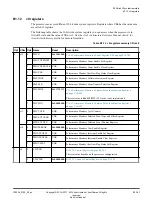
Page 174: ...ccess to internal memory on page C5 608 2 CDBGDR2 UNK Cache Debug Data Register 2 see C5 1 About direct access to internal memory on page C5 608 3 CDBGDR3 UNK Cache Debug Data Register 3 see C5 1 About direct access to internal memory on page C5 608 c2 0 CDBGDCT UNK Cache Debug Data Cache Tag Read Operation Register see C5 1 About direct access to internal memory on page C5 608 1 CDBGICT UNK Cache...

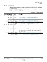
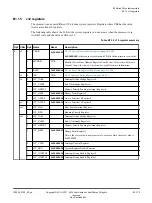
Page 175: ...ess Register on page B1 321 0 c14 CNTPCT UNK Physical Timer Count Register 1 c14 CNTVCT UNK Virtual Timer Count Register 2 c14 CNTP_CVAL UNK Physical Timer CompareValue Register 3 c14 CNTV_CVAL UNK Virtual Timer CompareValue Register 4 c14 CNTVOFF UNK Virtual Timer Offset Register 6 c14 CNTHP_CVAL UNK Physical Timer CompareValue Register 0 c15 CPUACTLR 0x00000000090CA000 B1 42 CPU Auxiliary Contro...

Page 176: ...herwise ID_DFR0 2 0x03010066 B1 73 Debug Feature Register 0 on page B1 267 Bits 19 16 are 0x1 if ETM is implemented and 0x0 otherwise ID_AFR0 3 0x00000000 B1 72 Auxiliary Feature Register 0 on page B1 266 ID_MMFR0 4 0x10201105 B1 80 Memory Model Feature Register 0 on page B1 281 ID_MMFR1 5 0x40000000 B1 81 Memory Model Feature Register 1 on page B1 283 ID_MMFR2 6 0x01260000 B1 82 Memory Model Feat...

Page 177: ...1 39 Cache Size ID Register on page B1 201 CLIDR 1 0x0A200023 B1 40 Cache Level ID Register on page B1 204 The value is 0x09200003 if the L2 cache is not implemented AIDR 7 0x00000000 B1 34 Auxiliary ID Register on page B1 196 CSSELR 2 c0 0 0x00000000 B1 45 Cache Size Selection Register on page B1 217 B1 AArch32 system registers B1 20 AArch32 Identification registers 100236_0100_00_en Copyright 20...

Page 178: ... copy of the register is 0x0 You must program the Non secure copy of the register with the required initial value as part of the processor boot sequence DACR c3 0 c0 0 UNK 32 bit B1 47 Domain Access Control Register on page B1 221 PRRR c10 0 c2 0 UNK 32 bit B1 101 Primary Region Remap Register on page B1 322 MAIR0 0 UNK 32 bit B1 95 Memory Attribute Indirection Registers 0 and 1 on page B1 310 NMR...

Page 179: ...liary Instruction Fault Status Register on page B1 197 DFAR c6 0 c0 0 UNK Data Fault Address Register see the Arm Architecture Reference Manual Armv8 for Armv8 A architecture profile IFAR 2 UNK Instruction Fault Address Register see the Arm Architecture Reference Manual Armv8 for Armv8 A architecture profile The Virtualization registers include additional fault handling registers See B1 28 AArch32...

Page 180: ... B1 32 Auxiliary Control Register on page B1 193 CPACR 2 0x00000000 B1 41 Architectural Feature Access Control Register on page B1 206 FCSEIDR c13 0 c0 0 0x00000000 B1 53 FCSE Process ID Register on page B1 229 B1 AArch32 system registers B1 23 AArch32 Other System control registers 100236_0100_00_en Copyright 2015 2017 2019 Arm Limited or its affiliates All rights reserved B1 180 Non Confidential...

Page 181: ... profile for more information Table B1 23 Address translation operations Name CRn Op1 CRm Op2 Reset Width Description PAR c7 0 c4 0 UNK 32 bit B1 100 Physical Address Register on page B1 321 0 c7 64 bit B1 AArch32 system registers B1 24 AArch32 Address registers 100236_0100_00_en Copyright 2015 2017 2019 Arm Limited or its affiliates All rights reserved B1 181 Non Confidential ...

Page 182: ...tructions Name CRn Op1 CRm Op2 Reset Description TPIDRURW c13 0 c0 2 UNK User Read Write Thread ID Register TPIDRURO 3 UNK User Read Only Thread ID Register TPIDRPRW 4 UNK EL1 only Thread ID Register HTPIDR 4 c0 2 UNK Hyp Software Thread ID Register B1 AArch32 system registers B1 25 AArch32 Thread registers 100236_0100_00_en Copyright 2015 2017 2019 Arm Limited or its affiliates All rights reserve...

Page 183: ... 0x6FFFBFFF C10 3 Performance Monitors Common Event Identification Register 0 on page C10 695 The reset value is 0x6E3FBFFF if L2 cache is not implemented PMCEID1 7 0x00000000 C10 4 Performance Monitors Common Event Identification Register 1 on page C10 699 PMCCNTR c13 0 UNK Performance Monitors Cycle Count Register PMXEVTYPER 1 UNK Performance Monitors Selected Event Type Register PMXEVCNTR 2 UNK...

Page 184: ...TR5 5 UNK PMEVTYPER0 c12 0 UNK Performance Monitors Selected Event Type Register 0 PMEVTYPER1 1 UNK PMEVTYPER2 2 UNK PMEVTYPER3 3 UNK PMEVTYPER4 4 UNK PMEVTYPER5 5 UNK PMCCFILTR c15 7 0x00000000 Performance Monitors Cycle Count Filter Register B1 AArch32 system registers B1 26 AArch32 Performance monitor registers 100236_0100_00_en Copyright 2015 2017 2019 Arm Limited or its affiliates All rights ...

Page 185: ...le Register NSACR 2 0x00000000 B1 98 Non Secure Access Control Register on page B1 317 If EL3 is AArch64 then the NSACR reads as 0x00000C00 VBAR c12 0 c0 0 0x00000000 B1 119 Vector Base Address Register on page B1 354 0x00000000 is the secure reset value and UNK is the non secure reset value MVBAR 1 UNK Monitor Vector Base Address Register ISR c1 0 UNK Interrupt Status Register B1 AArch32 system r...

Page 186: ...figuration If Advanced SIMD and floating point are implemented the reset value is 0x000033FF If Advanced SIMD and floating point are not implemented the reset value is 0x0000BFFF HSTR 3 0x00000000 32 bit Hypervisor System Trap Register HTCR c2 4 c0 2 UNK 32 bit B1 70 Hyp Translation Control Register on page B1 263 VTCR c1 2 UNK 32 bit Virtualization Translation Control Register HTTBR 4 c2 UNK 64 b...

Page 187: ...0 0x00000000 32 bit B1 58 Hyp Auxiliary Memory Attribute Indirection Register 0 on page B1 235 HAMAIR1 1 0x00000000 32 bit B1 59 Hyp Auxiliary Memory Attribute Indirection Register 1 on page B1 236 HVBAR c12 4 c0 0 UNK 32 bit Hyp Vector Base Address Register B1 AArch32 system registers B1 28 AArch32 Virtualization registers 100236_0100_00_en Copyright 2015 2017 2019 Arm Limited or its affiliates A...

Page 188: ...RO 32 bit Interrupt Acknowledge Register 1 ICC_EOIR1 1 WO 32 bit End Of Interrupt Register 1 ICC_HPPIR1 2 RO 32 bit Highest Priority Pending Interrupt Register 1 ICC_BPR1 3 RW 0x00000003 32 bit Binary Point Register 1 This is the reset value in non secure state In secure state the reset value is 0x00000002 ICC_CTLR 4 RW 0x00000400 32 bit Interrupt Control Register ICC_SRE 5 RW 0x00000000 32 bit Sy...

Page 189: ...er 2 ICH_LR3 3 RW 0x00000000 32 bit Interrupt Controller List Register 3 ICH_LRC0 c14 0 RW 0x00000000 32 bit Interrupt Controller List Register 0 ICH_LRC1 1 RW 0x00000000 32 bit Interrupt Controller List Register 1 ICH_LRC2 2 RW 0x00000000 32 bit Interrupt Controller List Register 2 ICH_LRC3 3 RW 0x00000000 32 bit Interrupt Controller List Register 3 ICC_MCTLR 6 c12 4 RW 0x00000400 32 bit Interrup...

Page 190: ...scribed in B4 2 AArch32 Generic Timer register summary on page B4 571 See also the Arm Architecture Reference Manual Armv8 for Armv8 A architecture profile for more information B1 AArch32 system registers B1 30 AArch32 Generic Timer registers 100236_0100_00_en Copyright 2015 2017 2019 Arm Limited or its affiliates All rights reserved B1 190 Non Confidential ...

Page 191: ... on page C5 608 for information on how these registers are used CDBGDR1 1 UNK 32 bit Data Register 1 see C5 1 About direct access to internal memory on page C5 608 CDBGDR2 2 UNK 32 bit Data Register 2 see C5 1 About direct access to internal memory on page C5 608 CDBGDR3 3 UNK 32 bit Data Register 3 see C5 1 About direct access to internal memory on page C5 608 CDBGDCT c2 0 UNK 32 bit Data Cache T...

Page 192: ...000000 64 bit B1 43 CPU Extended Control Register on page B1 212 CPUMERRSR 2 c15 64 bit B1 44 CPU Memory Error Syndrome Register on page B1 214 L2MERRSR 3 c15 64 bit B1 94 L2 Memory Error Syndrome Register on page B1 307 B1 AArch32 system registers B1 31 AArch32 Implementation defined registers 100236_0100_00_en Copyright 2015 2017 2019 Arm Limited or its affiliates All rights reserved B1 192 Non ...

Page 193: ...TLR access control L2CTLR access control CPUECTLR access control CPUACTLR access control Figure B1 1 ACTLR bit assignments 31 7 Reserved RES0 L2ACTLR access control 6 L2ACTLR write access control The possible values are 0 The register is not write accessible from a lower exception level This is the reset value 1 The register is write accessible from EL2 L2ECTLR access control 5 L2ECTLR write acces...

Page 194: ...le values are 0 The register is not write accessible from a lower exception level This is the reset value 1 The register is write accessible from EL2 To access the ACTLR MRC p15 0 Rt c1 c0 1 Read ACTLR into Rt MCR p15 0 Rt c1 c0 1 Write Rt to ACTLR Register access is encoded as follows Table B1 30 ACTLR access encoding coproc opc1 CRn CRm opc2 1111 000 0001 0000 001 B1 AArch32 system registers B1 ...

Page 195: ...e processor does not implement ADFSR This register is always RES0 B1 AArch32 system registers B1 33 Auxiliary Data Fault Status Register 100236_0100_00_en Copyright 2015 2017 2019 Arm Limited or its affiliates All rights reserved B1 195 Non Confidential ...

Page 196: ...e processor does not implement AIDR This register is always RES0 B1 AArch32 system registers B1 34 Auxiliary ID Register 100236_0100_00_en Copyright 2015 2017 2019 Arm Limited or its affiliates All rights reserved B1 196 Non Confidential ...

Page 197: ...e processor does not implement AIFSR This register is always RES0 B1 AArch32 system registers B1 35 Auxiliary Instruction Fault Status Register 100236_0100_00_en Copyright 2015 2017 2019 Arm Limited or its affiliates All rights reserved B1 197 Non Confidential ...

Page 198: ...e processor does not implement AMAIR0 This register is always RES0 B1 AArch32 system registers B1 36 Auxiliary Memory Attribute Indirection Register 0 100236_0100_00_en Copyright 2015 2017 2019 Arm Limited or its affiliates All rights reserved B1 198 Non Confidential ...

Page 199: ...e processor does not implement AMAIR1 This register is always RES0 B1 AArch32 system registers B1 37 Auxiliary Memory Attribute Indirection Register 1 100236_0100_00_en Copyright 2015 2017 2019 Arm Limited or its affiliates All rights reserved B1 199 Non Confidential ...

Page 200: ...emented with the GIC CPU interface the input PERIPHBASE 31 18 determines the reset value If the GIC CPU interface is not implemented this field is RAZ 17 8 Reserved RES0 PERIPHBASE 39 32 7 0 If the processor is implemented with the GIC CPU interface the input PERIPHBASE 39 32 determines the reset value If the GIC CPU interface is not implemented this field is RAZ To access the CBAR MRC p15 1 Rt c1...

Page 201: ... is one copy of this register that is used in both Secure and Non secure states The implementation includes one CCSIDR for each cache that it can access CSSELR selects which Cache Size ID Register is accessible Attributes CCSIDR is a 32 bit register WB 31 28 27 12 3 0 RA LineSize WT 30 29 13 2 WA NumSets Associativity Figure B1 3 CCSIDR bit assignments WT 31 Indicates support for Write Through 0 C...

Page 202: ...individual bit field and complete register encodings for the CCSIDR The CSSELR determines which CCSIDR to select Table B1 32 CCSIDR encodings CSSELR Cache Size Complete register encoding Register bit field encoding WT WB RA WA NumSets Associativity LineSize 0x0 L1 Data cache 8KB 0x7003E01A 0 1 1 1 0x001F 0x003 0x2 16KB 0x7007E01A 0x003F 0x003 0x2 32KB 0x700FE01A 0x007F 0x003 0x2 64KB 0x701FE01A 0x...

Page 203: ...ncoding coproc opc1 CRn CRm opc2 1111 001 0000 0000 000 B1 AArch32 system registers B1 39 Cache Size ID Register 100236_0100_00_en Copyright 2015 2017 2019 Arm Limited or its affiliates All rights reserved B1 203 Non Confidential ...

Page 204: ...ES0 Figure B1 4 CLIDR bit assignments ICB 31 30 Inner cache boundary This field indicates the boundary between the inner and the outer domain 0b00 Not disclosed in this mechanism LoUU 29 27 Indicates the Level of Unification Uniprocessor for the cache hierarchy 0b001 L1 cache is the last level of cache that must be cleaned or invalidated when cleaning or invalidating to the point of unification fo...

Page 205: ...m Ctype1 upwards after it has seen a value of 0b000 no caches exist at further out levels of the hierarchy So for example if Ctype2 is the first Cache Type field with a value of 0b000 the value of Ctype3 must be ignored Ctype2 5 3 Indicates the type of cache if the processor implements L2 cache 0b000 L2 cache is not implemented 0b100 L2 cache is implemented as a unified cache Ctype1 2 0 Indicates ...

Page 206: ...DIS 31 Disable Advanced SIMD functionality 0 Does not cause any instructions to be UNDEFINED This is the reset value 1 All instruction encodings that are part of Advanced SIMD but that are not floating point instructions are UNDEFINED If Advanced SIMD and floating point are not implemented this bit is RES0 30 24 Reserved RES0 cp11 23 22 Defines the access rights for CP11 that control the Advanced ...

Page 207: ...truction exception This is the reset value 0b01 Access at EL1 only Any attempt to access Advanced SIMD and floating point registers or instructions from software executing at EL0 generates an Undefined Instruction exception 0b10 Reserved 0b11 Full access If Advanced SIMD and floating point are not implemented this bit is RES0 The Advanced SIMD and floating point features controlled by these fields...

Page 208: ...t you do not modify this register unless directed by Arm Configurations CPUACTLR is Common to the Secure and Non secure states Mapped to the AArch64 CPUACTLR_EL1 register See B2 36 CPU Auxiliary Control Register EL1 on page B2 412 Attributes CPUACTLR is a 64 bit register 31 22 18 17 0 9 10 11 12 13 15 16 19 20 21 28 29 RES0 DIDIS RES0 L1PCTL L1RADIS RADIS NPFSTRM DSTDIS STRIDE 63 CDIDIS 30 23 24 S...

Page 209: ...cutive streaming cache line does not allocate in the L1 or L2 cache 0b11 Disables streaming All write allocate lines allocate in the L1 or L2 cache L1RADIS 26 25 Write streaming no L1 allocate threshold The possible values are 0b00 4th consecutive streaming cache line does not allocate in the L1 cache This is the reset value 0b01 64th consecutive streaming cache line does not allocate in the L1 ca...

Page 210: ...strides to trigger prefetch This is the reset value 1 3 consecutive strides to trigger prefetch 16 Reserved RES0 L1PCTL 15 13 L1 Data prefetch control The value of the this field determines the maximum number of outstanding data prefetches allowed in the L1 memory system excluding those generated by software load or PLD instructions The possible values are 0b000 Prefetch disabled 0b001 1 outstandi...

Page 211: ... errors are not injected This is the reset value 1 Double bit errors are injected on all writes to the L1 D cache data RAMs for the first word of each 32 byte region 5 0 Reserved RES0 To access the CPUACTLR MRRC p15 0 Rt Rt2 c15 Read CPU Auxiliary Control Register MCRR p15 0 Rt Rt2 c15 Write CPU Auxiliary Control Register Register access is encoded as follows Table B1 36 CPUACTLR access encoding c...

Page 212: ...th other cores in the cluster This is the reset value 1 Enables data coherency with other cores in the cluster Set the SMPEN bit before enabling the caches even if there is only one core in the system FPRETCTL 5 3 Advanced SIMD and floating point retention control The possible values are 0b000 Disable the retention circuit This is the reset value 0b001 2 Architectural Timer ticks are required befo...

Page 213: ...y 0b100 64 Architectural Timer ticks are required before retention entry 0b101 128 Architectural Timer ticks are required before retention entry 0b110 256 Architectural Timer ticks are required before retention entry 0b111 512 Architectural Timer ticks are required before retention entry To access the CPUECTLR MRRC p15 1 Rt Rt2 c15 Read CPU Extended Control Register MCRR p15 1 Rt Rt2 c15 Write CPU...

Page 214: ...ERRSR is a 64 bit register 24 23 21 20 Other error count Repeat error count 31 32 0 63 RES0 47 48 40 39 30 Valid RAMID 18 17 RES0 CPUID Way RAM address Fatal RES0 12 11 62 Figure B1 8 CPUMERRSR bit assignments Fatal 63 Fatal bit This bit is set to 1 on the first memory error that caused a data abort It is a sticky bit so that after it is set it remains set until the register is written The reset v...

Page 215: ... memory error The possible values are 0x00 L1 Instruction tag RAM 0x01 L1 Instruction data RAM 0x08 L1 Data tag RAM 0x09 L1 Data data RAM 0x0A L1 Data dirty RAM 0x18 TLB RAM 23 21 Reserved RES0 CPUID Way 20 18 Indicates the RAM where the first memory error occurred L1 I tag RAM 0x0 Way 0 0x1 Way 1 0x2 0x7 Unused L1 I data RAM 0x0 Bank 0 0x1 Bank 1 0x2 0x7 Unused TLB RAM 0x0 Way 0 0x1 Way 1 0x2 0x7...

Page 216: ...y error events from different RAMs occur in the same cycle one of the errors is selected arbitrarily If two or more memory error events from different RAMs that do not match the RAMID Way and index information in this register while the sticky Valid bit is set occur in the same cycle then the Other error count field is incremented only by one To access the CPUMERRSR MRRC p15 2 Rt Rt2 c15 Read CPUM...

Page 217: ... mapped to AArch64 register CSSELR_EL1 See B2 34 Cache Size Selection Register EL1 on page B2 408 If EL3 is using AArch32 there are separate Secure and Non secure instances of this register Attributes CSSELR is a 32 bit register InD UNK SBZP 31 4 3 1 0 Level Figure B1 9 CSSELR bit assignments 31 4 Reserved RES0 Level 3 1 Cache level of required cache 0b000 L1 0b001 L2 0b010 0b111 Reserved The comb...

Page 218: ... Register access is encoded as follows Table B1 39 CSSELR access encoding coproc opc1 CRn CRm opc2 1111 010 0000 0001 000 B1 AArch32 system registers B1 45 Cache Size Selection Register 100236_0100_00_en Copyright 2015 2017 2019 Arm Limited or its affiliates All rights reserved B1 218 Non Confidential ...

Page 219: ... 24 Cache Write Back granule Log2 of the number of words of the maximum size of memory that can be overwritten as a result of the eviction of a cache entry that has had a memory location in it modified 0x4 Cache Write Back granule size is 16 words ERG 23 20 Exclusives Reservation Granule Log2 of the number of words of the maximum size of the reservation granule that has been implemented for the Lo...

Page 220: ...instruction caches that the processor controls 0x4 Smallest instruction cache line size is 16 words To access the CTR MRC p15 0 Rt c0 c0 1 Read CTR into Rt Register access is encoded as follows Table B1 40 CTR access encoding coproc opc1 CRn CRm opc2 1111 010 0000 0000 001 B1 AArch32 system registers B1 46 Cache Type Register 100236_0100_00_en Copyright 2015 2017 2019 Arm Limited or its affiliates...

Page 221: ...ster 31 30 29 28 27 26 25 24 23 22 21 20 19 18 17 16 15 14 13 12 11 10 9 8 7 6 5 4 3 2 1 0 D15 D14 D13 D12 D11 D10 D9 D8 D7 D6 D5 D4 D3 D2 D1 D0 Figure B1 11 DACR bit assignments D n bits 2n 1 2n for n 0 to 15 31 0 Domain n access permission where n 0 to 15 Permitted values are 0b00 No access Any access to the domain generates a Domain fault 0b01 Client Accesses are checked against the permission ...

Page 222: ... on page B1 251 DFAR S is architecturally mapped to AArch64 register FAR_EL2 31 0 See B2 45 Fault Address Register EL2 on page B2 430 Attributes DFAR is a 32 bit register 31 0 VA of faulting address of synchronous Data Abort exception Figure B1 12 DFAR bit assignments VA 31 0 The Virtual Address of faulting address of synchronous Data Abort exception To access the DFAR MRC p15 0 Rt c6 c0 0 Read DF...

Page 223: ...64 register ESR_EL1 See B2 41 Exception Syndrome Register EL1 on page B2 423 If EL3 is using AArch32 there are separate Secure and Non secure instances of this register There are two formats for this register The current translation table format determines which format of the register is used Attributes DFSR is a 32 bit register B1 AArch32 system registers B1 49 Data Fault Status Register 100236_0...

Page 224: ...0 External abort marked as DECERR 1 External abort marked as SLVERR For aborts other than external aborts this bit always returns 0 WnR 11 Write not Read bit This field indicates whether the abort was caused by a write or a read access 0 Abort caused by a read access 1 Abort caused by a write access For faults on CP15 cache maintenance operations including the VA to PA translation operations this ...

Page 225: ...walk first level 0b01101 Permission fault section 0b01110 Synchronous external abort on translation table walk second level 0b01111 Permission fault second level 0b10000 TLB conflict abort 0b10101 LDREX or STREX abort 0b10110 Asynchronous external abort 0b11000 Asynchronous parity error on memory access 0b11001 Synchronous parity error on memory access 0b11100 Synchronous parity error on translati...

Page 226: ...lave error caused an abort 0 External abort marked as DECERR 1 External abort marked as SLVERR For aborts other than external aborts this bit always returns 0 WnR 11 Write not Read bit This field indicates whether the abort was caused by a write or a read access 0 Abort caused by a read access 1 Abort caused by a write access For faults on CP15 cache maintenance operations including the VA to PA t...

Page 227: ...n memory access on translation table walk first level LL bits indicate level 0b100001 Alignment fault 0b100010 Debug event 0b110000 TLB conflict abort 0b110101 LDREX or STREX abort Table B1 43 Encodings of LL bits associated with the MMU fault Bits Meaning 0b00 Reserved 0b01 Level 1 0b10 Level 2 0b11 Level 3 To access the DFSR MRC p15 0 Rt c5 c0 0 Read DFSR into Rt MCR p15 0 Rt c5 c0 0 Write Rt to...

Page 228: ...he COND field is not valid 1 The COND field is valid When an instruction is trapped CV is set to 1 COND ISS 23 20 The Condition field for the trapped instruction This field is valid only when CV is set to 1 If CV is set to 0 this field is RES0 When an instruction is trapped the COND field is set to the condition the instruction was executed with B1 AArch32 system registers B1 52 Encoding of ISS 24...

Page 229: ...es not implement Fast Context Switch Extension FCSE This register is always RES0 B1 AArch32 system registers B1 53 FCSE Process ID Register 100236_0100_00_en Copyright 2015 2017 2019 Arm Limited or its affiliates All rights reserved B1 229 Non Confidential ...

Page 230: ...e processor does not implement HACR This register is always RES0 B1 AArch32 system registers B1 54 Hyp Auxiliary Configuration Register 100236_0100_00_en Copyright 2015 2017 2019 Arm Limited or its affiliates All rights reserved B1 230 Non Confidential ...

Page 231: ...rol CPUACTLR access control Figure B1 15 HACTLR bit assignments 31 7 Reserved RES0 L2ACTLR access control 6 L2ACTLR write access control The possible values are 0 The register is not write accessible from Non secure EL1 This is the reset value 1 The register is write accessible from Non secure EL1 Write access from Non secure EL1 also requires ACTLR S 6 to be set L2ECTLR access control 5 L2ECTLR w...

Page 232: ...on secure EL1 also requires ACTLR S 1 to be set CPUACTLR access control 0 CPUACTLR write access control The possible values are 0 The register is not write accessible from Non secure EL1 This is the reset value 1 The register is write accessible from Non secure EL1 Write access from Non secure EL1 also requires ACTLR S 0 to be set To access the HACTLR MRC p15 4 Rt c1 c0 1 Read HACTLR into Rt MCR p...

Page 233: ...e processor does not implement HADFSR This register is always RES0 B1 AArch32 system registers B1 56 Hyp Auxiliary Data Fault Status Syndrome Register 100236_0100_00_en Copyright 2015 2017 2019 Arm Limited or its affiliates All rights reserved B1 233 Non Confidential ...

Page 234: ...e processor does not implement HAIFSR This register is always RES0 B1 AArch32 system registers B1 57 Hyp Auxiliary Instruction Fault Status Syndrome Register 100236_0100_00_en Copyright 2015 2017 2019 Arm Limited or its affiliates All rights reserved B1 234 Non Confidential ...

Page 235: ...e processor does not implement HAMAIR0 This register is always RES0 B1 AArch32 system registers B1 58 Hyp Auxiliary Memory Attribute Indirection Register 0 100236_0100_00_en Copyright 2015 2017 2019 Arm Limited or its affiliates All rights reserved B1 235 Non Confidential ...

Page 236: ...e processor does not implement HAMAIR1 This register is always RES0 B1 AArch32 system registers B1 59 Hyp Auxiliary Memory Attribute Indirection Register 1 100236_0100_00_en Copyright 2015 2017 2019 Arm Limited or its affiliates All rights reserved B1 236 Non Confidential ...

Page 237: ...rally mapped to AArch64 register CPTR_EL2 See B2 32 Architectural Feature Trap Register EL2 on page B2 404 Attributes HCPTR is a 32 bit register RES1 31 30 21 20 19 16 15 14 13 12 11 10 9 8 7 6 5 4 3 2 1 0 RES0 TCPAC RES0 TTA TASE TCP11 TCP10 RES1 RES0 Figure B1 16 HCPTR bit assignments TCPAC 31 Trap CPACR accesses The possible values of this bit are 0 Has no effect on CPACR accesses 1 Trap valid ...

Page 238: ... mode Hyp mode generates an Undefined Instruction exception taken in Hyp mode Resets to 0 If the TCP11 and TCP10 fields are set to different values the behavior is the same as if both fields were set to the value of TCP10 in all respects other than the value read back by explicitly reading TCP11 TCP10 10 Trap CP10 The possible values of each of this bit is 0 If NSACR cp10 is set to 1 then Hyp mode...

Page 239: ...ter access is encoded as follows Table B1 45 HCPTR access encoding coproc opc1 CRn CRm opc2 1111 100 0001 0001 010 B1 AArch32 system registers B1 60 Hyp Architectural Feature Trap Register 100236_0100_00_en Copyright 2015 2017 2019 Arm Limited or its affiliates All rights reserved B1 239 Non Confidential ...

Page 240: ... 22 21 20 19 18 17 16 15 14 13 12 11 10 9 8 7 6 5 4 3 2 1 TRVM RES0 VM SWIO PTW FMO IMO AMO VF VI VA FB BSU DC TWI TWE TID0 HCD RES0 TGE TVM TTLB TPU TSW TAC TIDCP TSC TID3 TID2 TID1 TPC Figure B1 17 HCR bit assignments 31 Reserved RES0 TRVM 30 Trap Read of Virtual Memory controls When 1 this causes Reads to the EL1 virtual memory control registers from EL1 to be trapped to EL2 This covers the fol...

Page 241: ...ory controls When 1 this causes Writes to the EL1 virtual memory control registers from EL1 to be trapped to EL2 This covers the following registers SCTLR TTBR0 TTBR1 TTBCR DACR DFSR IFSR DFAR IFAR ADFSR AIFSR PRRR MAIR0 NMRR MAIR1 AMAIR0 AMAIR1 and CONTEXTIDR The reset value is 0 TTLB 25 Trap TLB maintenance instructions When 1 this causes TLB maintenance instructions executed from EL1 that are n...

Page 242: ...code1 is 0 to 7 CRm is c0 c1 c2 c5 c6 c7 c8 opcode2 is 0 to 7 CRn is 10 Opcode1 is 0 to 7 CRm is c0 c1 c4 c8 opcode2 is 0 to 7 CRn is 11 Opcode1 is 0 to 7 CRm is c0 to c8 or c15 opcode2 is 0 to 7 Accesses from EL0 are UNDEFINED Resets to 0 TSC 19 Trap SMC instruction When this bit is set to 1 any attempt from a Non secure EL1 state to execute an SMC instruction that passes its condition check if i...

Page 243: ...I 13 Trap WFI When 1 this causes the WFI instruction executed from EL1 or EL0 to be trapped to EL2 if the instruction would otherwise cause suspension of execution For example if there is not a pending WFI wake up event The reset value is 0 DC 12 Default cacheable When this bit is set to 1 and the Non secure EL1 and EL0 stage 1 MMU is disabled the memory type and attributes determined by the stage...

Page 244: ...al FIQ exception to the Guest OS when the processor is executing in Non secure state at EL0 or EL1 The Guest OS cannot distinguish the virtual exception from the corresponding physical exception The reset value is 0 AMO 5 Asynchronous Abort Mask Override When this is set to 1 it overrides the effect of CPSR A and enables virtual exception signaling by the VA bit The reset value is 0 IMO 4 IRQ Mask...

Page 245: ...ond stage of translation for execution in EL1 and EL0 The reset value is 0 To access the HCR MRC p15 4 Rt c1 c1 0 Read Hyp Configuration Register MCR p15 4 Rt c1 c1 0 Write Hyp Configuration Register Register access is encoded as follows Table B1 46 HCR access encoding coproc opc1 CRn CRm opc2 1111 100 0001 0001 000 B1 AArch32 system registers B1 61 Hyp Configuration Register 100236_0100_00_en Cop...

Page 246: ...translation regime The possible values are 0 No effect on the stage 2 of the EL1 EL0 translation regime for instruction accesses 1 Forces all stage 2 translations for instruction accesses to Normal memory to be Non cacheable for the EL0 EL1 translation regime CD 0 Stage 2 Data cache disable When HCR VM is 1 this forces all stage 2 translations for data accesses and translation table walks to Norma...

Page 247: ...Register access is encoded as follows Table B1 47 HCR2 access encoding coproc opc1 CRn CRm opc2 1111 100 0001 0001 100 B1 AArch32 system registers B1 62 Hyp Configuration Register 2 100236_0100_00_en Copyright 2015 2017 2019 Arm Limited or its affiliates All rights reserved B1 247 Non Confidential ...

Page 248: ...OSA TDA TDE HPME TPM TPMCR 12 TDRA Figure B1 19 HDCR bit assignments 31 12 Reserved RES0 TDRA 11 Trap debug ROM address register access 0 Has no effect on accesses to debug ROM address registers from EL1 and EL0 1 Trap valid Non secure EL1 and EL0 access to debug ROM address registers to Hyp mode When this bit is set to 1 any valid Non secure access to the following registers is trapped to Hyp mod...

Page 249: ...e Non secure Debug exceptions to Hyp mode When this bit is set to 1 any Debug exception taken in Non secure state is trapped to Hyp mode If HCR TGE is 1 then this bit is ignored and treated as though it is 1 other than for the value read back from HDCR This bit resets to 0 HPME 7 Hypervisor Performance Monitor Enable 0 Hyp mode performance monitor counters disabled 1 Hyp mode performance monitor c...

Page 250: ...nter is accessible only from EL2 The HPME bit enables access to the counters in this range If this field is set to 0 or to a value larger than PMCR N then the behavior in Non secure EL0 and EL1 is CONSTRAINED UNPREDICTABLE and one of the following must happen The number of counters accessible is an UNKNOWN non zero value less than PMCR N There is no access to any counters For reads of HDCR HPMN by...

Page 251: ...0 HDFAR S is architecturally mapped to AArch32 register DFAR S See B1 48 Data Fault Address Register on page B1 222 Attributes HDFAR is a 32 bit register 31 0 VA of faulting address of synchronous Data Abort exception Figure B1 20 HDFAR bit assignments VA 31 0 The Virtual Address of faulting address of synchronous Data Abort exception To access the HDFAR MRC p15 4 Rt c6 c0 0 Read HDFAR into Rt MCR...

Page 252: ...rchitecturally mapped to AArch32 register IFAR S See B1 86 Instruction Fault Address Register on page B1 293 Attributes HIFAR is a 32 bit register 31 0 VA of faulting address of synchronous Prefetch Abort exception Figure B1 21 HIFAR bit assignments VA 31 0 The Virtual Address of faulting address of synchronous Prefetch Abort exception To access the HIFAR MRC p15 4 Rt c6 c0 2 Read HIFAR into Rt MC...

Page 253: ...pervisor IPA Fault Address Register EL2 on page B2 440 Attributes HPFAR is a 32 bit register 31 0 FIPA 39 12 4 3 RES0 Figure B1 22 HPFAR bit assignments FIPA 39 12 31 4 Bits 39 12 of the faulting intermediate physical address 3 0 Reserved RES0 To access the HPFAR MRC p15 4 Rt c6 c0 4 Read HPFAR into Rt MCR p15 4 Rt c6 c0 4 Write Rt to HPFAR Register access is encoded as follows Table B1 51 HPFAR a...

Page 254: ...7 6 3 2 1 0 TE RES1 EE FI I RES1 C A WXN RES0 RES0 9 RES0 SED 8 ITD RES1 5 4 CP15BEN RES0 27 28 23 17 16 15 14 10 RES1 RES1 RES0 Figure B1 23 HSCTLR bit assignments 31 Reserved RES0 TE 30 Thumb Exception enable This bit controls whether exceptions taken in Hyp mode are taken in A32 or T32 state 0 Exceptions taken in A32 state 1 Exceptions taken in T32 state 29 28 Reserved RES1 27 26 Reserved RES0 ...

Page 255: ... enable bit for instruction caches at EL2 0 Instruction caches disabled at EL2 If HSCTLR M is set to 0 instruction accesses from stage 1 of the EL2 translation regime are to Normal memory Outer Shareable Inner Non cacheable Outer Non cacheable 1 Instruction caches enabled at EL2 If HSCTLR M is set to 0 instruction accesses from stage 1 of the EL2 translation regime are to Normal memory Outer Share...

Page 256: ...an enable bit for data and unified caches at EL2 0 Data and unified caches disabled at EL2 1 Data and unified caches enabled at EL2 When this bit is 0 all EL2 Normal memory data accesses and all accesses to the EL2 translation tables are Non cacheable If this register is at the highest exception level implemented field resets to 0 Otherwise its reset value is UNKNOWN A 1 Alignment check enable Thi...

Page 257: ...EL2 stage 1 MMU enabled If this register is at the highest exception level implemented field resets to 0 Otherwise its reset value is UNKNOWN To access the HSCTLR MRC p15 4 Rt c1 c0 0 Read HSCTLR into Rt MCR p15 4 Rt c1 c0 0 Write Rt to HSCTLR Register access is encoded as follows Table B1 52 HSCTLR access encoding coproc opc1 CRn CRm opc2 1111 100 0001 0000 000 B1 AArch32 system registers B1 67 H...

Page 258: ...e exception class for the exception that is taken in Hyp mode See the Arm Architecture Reference Manual Armv8 for Armv8 A architecture profile for more information IL 25 Instruction length See the Arm Architecture Reference Manual Armv8 for Armv8 A architecture profile for more information ISS 24 0 Instruction specific syndrome See the Arm Architecture Reference Manual Armv8 for Armv8 A architectu...

Page 259: ... EL2 or EL3 Attributes HSTR is a 32 bit register 31 0 RES0 1 2 3 4 5 6 7 8 9 10 11 12 13 14 15 16 17 TTEE RES0 T15 T13 T12 T11 T10 T9 T8 T0 T1 T2 T3 RES0 T5 T6 T7 Figure B1 25 HSTR bit assignments 31 17 Reserved RES0 TTEE 16 Trap T32EE This value is 0 T32EE is not supported T15 15 Trap coprocessor primary register CRn 15 The possible values are 0 Has no effect on Non secure accesses to CP15 regist...

Page 260: ...ter CRn 10 The possible values are 0 Has no effect on Non secure accesses to CP15 registers 1 Trap valid Non secure accesses to coprocessor primary register CRn 10 to Hyp mode The reset value is 0 T9 9 Trap coprocessor primary register CRn 9 The possible values are 0 Has no effect on Non secure accesses to CP15 registers 1 Trap valid Non secure accesses to coprocessor primary register CRn 9 to Hyp...

Page 261: ... is 0 T2 2 Trap coprocessor primary register CRn 2 The possible values are 0 Has no effect on Non secure accesses to CP15 registers 1 Trap valid Non secure accesses to coprocessor primary register CRn 2 to Hyp mode The reset value is 0 T1 1 Trap coprocessor primary register CRn 1 The possible values are 0 Has no effect on Non secure accesses to CP15 registers 1 Trap valid Non secure accesses to co...

Page 262: ...oding coproc opc1 CRn CRm opc2 1111 100 0001 0001 011 B1 AArch32 system registers B1 69 Hyp System Trap Register 100236_0100_00_en Copyright 2015 2017 2019 Arm Limited or its affiliates All rights reserved B1 262 Non Confidential ...

Page 263: ...7 12 11 14 13 10 9 T0SZ IRGN0 0 31 ORGN0 SH0 RES0 3 2 30 24 23 22 RES0 RES1 RES1 RES0 Figure B1 26 HTCR bit assignments 31 Reserved RES1 30 24 Reserved RES0 23 Reserved RES1 22 14 Reserved RES0 SH0 13 12 Shareability attribute for memory associated with translation table walks using TTBR0 The possible values are 0b00 Non shareable 0b01 Reserved 0b10 Outer shareable 0b11 Inner shareable ORGN0 11 10...

Page 264: ...ormal memory Inner Write Back no Write Allocate Cacheable 7 3 Reserved RES0 T0SZ 2 0 Size offset of the memory region addressed by TTBR0 The region size is 2 32 TSIZE bytes The processor does not use the implementation defined bit HTCR 30 so this bit is RES0 To access the HTCR MRC p15 4 Rt c2 c0 2 Read HTCR into Rt MCR p15 4 Rt c2 c0 2 Write Rt to HTCR Register access is encoded as follows Table B...

Page 265: ...ector Base Address 4 5 Figure B1 27 HVBAR bit assignments Vector Base Address 31 5 Bits 31 5 of the base address of the exception vectors for exceptions taken in this exception level Bits 4 0 of an exception vector are the exception offset 4 0 Reserved RES0 To access the HVBAR MRC p15 4 Rt c12 c0 0 Read HVBAR into Rt MCR p15 4 Rt c12 c0 0 Write Rt to HVBAR Register access is encoded as follows Tab...

Page 266: ...e processor does not implement ID_AFR0 This register is always RES0 B1 AArch32 system registers B1 72 Auxiliary Feature Register 0 100236_0100_00_en Copyright 2015 2017 2019 Arm Limited or its affiliates All rights reserved B1 266 Non Confidential ...

Page 267: ...Figure B1 28 ID_DFR0 bit assignments 31 28 Reserved RES0 PerfMon 27 24 Indicates support for performance monitor model 0x3 Support for Performance Monitor Unit version 3 PMUv3 system registers MProfDbg 23 20 Indicates support for memory mapped debug model for M profile processors 0x0 Processor does not support M profile Debug architecture MMapTrc 19 16 Indicates support for memory mapped trace mod...

Page 268: ... Processor supports v8 Debug architecture with CP14 access To access the ID_DFR0 MRC p15 0 Rt c0 c1 2 Read ID_DFR0 into Rt Register access is encoded as follows Table B1 56 ID_DFR0 access encoding coproc opc1 CRn CRm opc2 1111 000 0000 0001 010 B1 AArch32 system registers B1 73 Debug Feature Register 0 100236_0100_00_en Copyright 2015 2017 2019 Arm Limited or its affiliates All rights reserved B1 ...

Page 269: ... 57 AArch32 Instruction Set Attribute Register 0 EL1 on page B2 455 There is one copy of this register that is used in both Secure and Non secure states Attributes ID_ISAR0 is a 32 bit register 31 28 27 24 23 20 19 16 15 12 11 8 7 4 3 0 RES0 Divide Debug Coproc CmpBranch Bitfield BitCount Swap Figure B1 29 ID_ISAR0 bit assignments 31 28 Reserved RES0 Divide 27 24 Indicates the implemented Divide i...

Page 270: ...wap 3 0 Indicates the implemented Swap instructions in the A32 instruction set 0x0 None implemented To access the ID_ISAR0 MRC p15 0 Rt c0 c2 0 Read ID_ISAR0 into Rt Register access is encoded as follows Table B1 57 ID_ISAR0 access encoding coproc opc1 CRn CRm opc2 1111 000 0000 0010 000 B1 AArch32 system registers B1 74 Instruction Set Attribute Register 0 100236_0100_00_en Copyright 2015 2017 20...

Page 271: ...egister 1 EL1 on page B2 457 There is one copy of this register that is used in both Secure and Non secure states Attributes ID_ISAR1 is a 32 bit register 31 28 27 24 23 20 19 16 15 12 11 8 7 4 3 0 Jazelle Interwork Immediate IfThen Extend Except_AR Except Endian Figure B1 30 ID_ISAR1 bit assignments Jazelle 31 28 Indicates the implemented Jazelle state instructions 0x1 The BXJ instruction and the...

Page 272: ... implemented A profile exception handling instructions 0x1 The SRS and RFE instructions and the A profile forms of the CPS instruction Except 7 4 Indicates the implemented exception handling instructions in the A32 instruction set 0x1 The LDM exception return LDM user registers and STM user registers instruction versions Endian 3 0 Indicates the implemented Endian instructions 0x1 The SETEND instr...

Page 273: ... register that is used in both Secure and Non secure states Attributes ID_ISAR2 is a 32 bit register 31 28 27 24 23 20 19 16 15 12 11 8 7 4 3 0 MultiAccessInt Reversal PSR_AR MultU MultS Mult MemHint LoadStore Figure B1 31 ID_ISAR2 bit assignments Reversal 31 28 Indicates the implemented Reversal instructions 0x2 The REV REV16 and REVSH instructions The RBIT instruction PSR_AR 27 24 Indicates the ...

Page 274: ...ptible multi access instructions 0x0 No support This means the LDM and STM instructions are not interruptible MemHint 7 4 Indicates the implemented memory hint instructions 0x4 The PLD instruction The PLI instruction The PLDW instruction LoadStore 3 0 Indicates the implemented additional load store instructions 0x2 The LDRD and STRD instructions The Load Acquire LDAB LDAH LDA LDAEXB LDAEXH LDAEX a...

Page 275: ... of this register that is used in both Secure and Non secure states Attributes ID_ISAR3 is a 32 bit register TabBranch 31 28 27 24 23 20 19 16 15 12 11 8 7 4 3 0 ThumbCopy SVC Saturate ThumbEE SynchPrim SIMD TrueNOP Figure B1 32 ID_ISAR3 bit assignments ThumbEE 31 28 Indicates the implemented Thumb Execution Environment T32EE instructions 0x0 None implemented TrueNOP 27 24 Indicates support for Tr...

Page 276: ...SAX SSAT16 SSUB16 SSUB8 SSAX SXTAB16 SXTB16 UADD16 UADD8 UASX UHADD16 UHADD8 UHASX UHSUB16 UHSUB8 UHSAX UQADD16 UQADD8 UQASX UQSUB16 UQSUB8 UQSAX USAD8 USADA8 USAT16 USUB16 USUB8 USAX UXTAB16 UXTB16 instructions and the GE 3 0 bits in the PSRs Saturate 3 0 Indicates the implemented Saturate instructions 0x1 The QADD QDADD QDSUB QSUB and the Q bit in the PSRs To access the ID_ISAR3 MRC p15 0 Rt c0 ...

Page 277: ...1 on page B2 463 There is one copy of this register that is used in both Secure and Non secure states Attributes ID_ISAR4 is a 32 bit register 31 24 23 20 19 16 15 12 11 8 7 4 3 0 SynchPrim_frac SWP_frac 28 27 PSR_M Barrier SMC Writeback WithShifts Unpriv Figure B1 33 ID_ISAR4 bit assignments SWP_frac 31 28 Indicates support for the memory system locking the bus for SWP or SWPB instructions 0x0 SW...

Page 278: ...e LSL 0 3 Support for other constant shift options both on load store and other instructions Support for register controlled shift options Unpriv 3 0 Indicates the implemented unprivileged instructions 0x2 The LDRBT LDRT STRBT and STRT instructions The LDRHT LDRSBT LDRSHT and STRHT instructions To access the ID_ISAR4 MRC p15 0 Rt c0 c2 4 Read ID_ISAR4 into Rt Register access is encoded as follows ...

Page 279: ...ribute Register 5 EL1 on page B2 465 There is one copy of this register that is used in both Secure and Non secure states Attributes ID_ISAR5 is a 32 bit register 31 12 11 8 7 0 RES0 SHA1 AES SEVL SHA2 4 3 16 15 20 19 CRC32 Figure B1 34 ID_ISAR5 bit assignments 31 20 Reserved RES0 CRC32 19 16 Indicates whether CRC32 instructions are implemented in AArch32 state 0x1 CRC32 instructions are implement...

Page 280: ...nd PMULL2 instructions operating on 64 bit data See the Cortex A35 Processor Cryptographic Extension Technical Reference Manual for more information SEVL 3 0 Indicates whether the SEVL instruction is implemented 0x1 SEVL implemented to send event local To access the ID_ISAR5 MRC p15 0 Rt c0 c2 5 Read ID_ISAR5 into Rt Register access is encoded as follows Table B1 62 ID_ISAR5 access encoding coproc...

Page 281: ...is used in both Secure and Non secure states Attributes ID_MMFR0 is a 32 bit register 31 12 11 8 7 0 OuterShr PMSA 4 3 28 27 24 23 20 19 16 15 FCSE AuxReg TCM ShareLvl VMSA InnerShr Figure B1 35 ID_MMFR0 bit assignments InnerShr 31 28 Indicates the innermost shareability domain implemented 0x1 Implemented with hardware coherency support FCSE 27 24 Indicates support for Fast Context Switch Extensio...

Page 282: ... VMSAv7 with support for remapping and the Access flag The PXN bit in the Short descriptor translation table format descriptors The Long descriptor translation table format To access the ID_MMFR0 MRC p15 0 Rt c0 c1 4 Read ID_MMFR0 into Rt Register access is encoded as follows Table B1 63 ID_MMFR0 access encoding coproc opc1 CRn CRm opc2 1111 000 0000 0001 100 B1 AArch32 system registers B1 80 Memo...

Page 283: ...and Non secure states Attributes ID_MMFR1 is a 32 bit register 31 12 11 8 7 0 BPred 4 3 28 27 2423 20 19 16 15 L1TstCln L1Uni L1Hvd L1UniSW L1HvdSW L1UniVA L1HvdVA Figure B1 36 ID_MMFR1 bit assignments BPred 31 28 Indicates branch predictor management requirements 0x4 For execution correctness branch predictor requires no flushing at any time L1TstCln 27 24 Indicates the supported L1 Data cache te...

Page 284: ... for a unified cache implementation 0x0 None supported L1HvdVA 3 0 Indicates the supported L1 cache line maintenance operations by MVA for a Harvard cache implementation 0x0 None supported To access the ID_MMFR1 MRC p15 0 Rt c0 c1 5 Read ID_MMFR1 into Rt Register access is encoded as follows Table B1 64 ID_MMFR1 access encoding coproc opc1 CRn CRm opc2 1111 000 0000 0001 101 B1 AArch32 system regi...

Page 285: ... used in both Secure and Non secure states Attributes ID_MMFR2 is a 32 bit register 31 12 11 8 7 0 HWAccFlg 4 3 28 27 24 23 20 19 16 15 WFIStall MemBarr UniTLB HvdTLB LL1HvdRng L1HvdBG L1HvdFG Figure B1 37 ID_MMFR2 bit assignments HWAccFlg 31 28 Hardware Access Flag Indicates support for a Hardware Access flag as part of the VMSAv7 implementation 0x0 Not supported WFIStall 27 24 Wait For Interrupt...

Page 286: ...vard TLB implementation 0x0 Not supported LL1HvdRng 11 8 L1 Harvard cache Range Indicates the supported L1 cache maintenance range operations for a Harvard cache implementation 0x0 Not supported L1HvdBG 7 4 L1 Harvard cache Background fetch Indicates the supported L1 cache background prefetch operations for a Harvard cache implementation 0x0 Not supported L1HvdFG 3 0 L1 Harvard cache Foreground fe...

Page 287: ...er 31 12 11 8 7 0 4 3 28 27 24 23 20 19 16 15 Reserved CohWalk CMemSz Supersec MaintBcst BPMaint CMaintSW CMaintVA Figure B1 38 ID_MMFR3 bit assignments Supersec 31 28 Supersections Indicates support for supersections 0x0 Supersections supported CMemSz 27 24 Cached Memory Size Indicates the size of physical memory supported by the processor caches 0x2 1TByte corresponding to a 40 bit physical addr...

Page 288: ... supported cache maintenance operations by MVA 0x1 Supported hierarchical cache maintenance operations by MVA are Invalidate data cache by MVA Invalidate data cache by MVA operations are treated as clean and invalidate data cache by MVA operations on the executing core If the operation is broadcast to another core then it is broadcast as an invalidate data cache by MVA operation Clean data cache b...

Page 289: ...gure B1 39 ID_PFR0 bit assignments 31 16 Reserved RES0 State3 15 12 Indicates support for Thumb Execution Environment T32EE instruction set This value is 0x0 Processor does not support the T32EE instruction set State2 11 8 Indicates support for Jazelle This value is 0x1 Processor supports trivial implementation of Jazelle State1 7 4 Indicates support for T32 instruction set This value is 0x3 Proce...

Page 290: ...ID_PFR0 access encoding coproc opc1 CRn CRm opc2 1111 000 0000 0001 000 B1 AArch32 system registers B1 84 Processor Feature Register 0 100236_0100_00_en Copyright 2015 2017 2019 Arm Limited or its affiliates All rights reserved B1 290 Non Confidential ...

Page 291: ... ID_PFR1 is a 32 bit register 31 12 11 8 7 0 GIC CPU 4 3 16 15 Virtualization 20 19 23 24 27 28 Reserved GenTimer MProgMod Security ProgMod Figure B1 40 ID_PFR1 bit assignments GIC CPU 31 28 GIC CPU support 0x0 GIC CPU interface is disabled GICCDISABLE is HIGH or not implemented 0x1 GIC CPU interface is implemented and enabled GICCDISABLE is LOW 27 20 Reserved RAZ GenTimer 19 16 Generic Timer supp...

Page 292: ...Supervisor Abort Undefined and System modes 0x1 Supported To access the ID_PFR1 MRC p15 0 Rt c0 c1 1 Read ID_PFR1 into Rt Register access is encoded as follows Table B1 68 ID_PFR1 access encoding coproc opc1 CRn CRm opc2 1111 000 0000 0001 001 B1 AArch32 system registers B1 85 Processor Feature Register 1 100236_0100_00_en Copyright 2015 2017 2019 Arm Limited or its affiliates All rights reserved ...

Page 293: ...IFAR S is architecturally mapped to AArch32 register HIFAR See B1 65 Hyp Instruction Fault Address Register on page B1 252 IFAR S is architecturally mapped to AArch64 register FAR_EL2 63 32 See B2 45 Fault Address Register EL2 on page B2 430 Attributes IFAR is a 32 bit register 31 0 VA of faulting address of synchronous Prefetch Abort exception Figure B1 41 IFAR bit assignments VA 31 0 The Virtual...

Page 294: ...4 register IFSR32_EL2 See B2 69 Instruction Fault Status Register EL2 on page B2 479 If EL3 is using AArch32 there are separate Secure and Non secure instances of this register Attributes IFSR is a 32 bit register There are two formats for this register The current translation table format determines which format of the register is used B1 AArch32 system registers B1 87 Instruction Fault Status Re...

Page 295: ...See bits 3 0 9 RAZ 8 5 Reserved RES0 FS 3 0 4 0 Fault Status bits This field indicates the type of exception generated Any encoding not listed is reserved 0b00010 Debug event 0b00011 Access flag fault section 0b00101 Translation fault section 0b00110 Access flag fault page 0b00111 Translation fault page 0b01000 Synchronous external abort non translation 0b01001 Domain fault section 0b01011 Domain ...

Page 296: ...b11110 Synchronous parity error on translation table walk second level B1 AArch32 system registers B1 88 IFSR with Short descriptor translation table format 100236_0100_00_en Copyright 2015 2017 2019 Arm Limited or its affiliates All rights reserved B1 296 Non Confidential ...

Page 297: ...ved RES0 Status 5 0 Fault Status bits This field indicates the type of exception generated Any encoding not listed is reserved 0b000000 Address size fault in TTBR0 or TTBR1 0b0001LL Translation fault LL bits indicate level 0b0010LL Access fault flag LL bits indicate level 0b0011LL Permission fault LL bits indicate level 0b010000 Synchronous external abort 0b0101LL Synchronous external abort on tra...

Page 298: ...R or HSR with the appropriate Fault Status code For such exceptions reported in the DFSR the corresponding IFSR is UNKNOWN To access the IFSR MRC p15 0 Rt c5 c0 1 Read IFSR into Rt MCR p15 0 Rt c5 c0 1 Write Rt to IFSR Register access is encoded as follows Table B1 70 IFSR access encoding coproc opc1 CRn CRm opc2 1111 000 0101 0000 001 B1 AArch32 system registers B1 89 IFSR with Long descriptor tr...

Page 299: ...ter that is used in both Secure and Non secure states Attributes ISR is a 32 bit register 31 9 8 7 6 5 0 RES0 F I A RES0 Figure B1 44 ISR bit assignments 31 9 Reserved RES0 A 8 External abort pending bit 0 No pending external abort 1 An external abort is pending I 7 IRQ pending bit Indicates whether an IRQ interrupt is pending 0 No pending IRQ 1 An IRQ interrupt is pending F 6 FIQ pending bit Indi...

Page 300: ... encoded as follows Table B1 71 ISR access encoding coproc opc1 CRn CRm opc2 1111 000 1100 0001 000 B1 AArch32 system registers B1 90 Interrupt Status Register 100236_0100_00_en Copyright 2015 2017 2019 Arm Limited or its affiliates All rights reserved B1 300 Non Confidential ...

Page 301: ...system has no outstanding ACP requests to the Cortex A35 processor When the L2 is idle the processor can update the L2ACTLR followed by an ISB After the L2ACTLR is updated the MMUs can be enabled and normal ACE and ACP traffic can resume Configurations There is one copy of this register that is used in both Secure and Non secure states L2ACTLR is mapped to the AArch64 L2ACTLR_EL1 register See B2 7...

Page 302: ...mplementations this field is RES0 13 4 Reserved RES0 Disable clean evict push to external 3 Disables clean evict push to external The possible values are 0 Enables clean evict to be pushed out to external This is the reset value for ACE 1 Disables clean evict from being pushed to external This is the reset value for CHI In AXI implementations this field is RES1 2 0 Reserved RES0 To access the L2AC...

Page 303: ...R is a 32 bit register 31 0 26 25 24 Reserved Number of cores RES0 23 1 L2 Data RAM input latency 22 21 20 Reserved CPU Cache Protection SCU L2 Cache Protection 4 5 6 L2 Data RAM output latency Reserved Figure B1 46 L2CTLR bit assignments 31 26 Reserved RES0 Number of cores 25 24 Number of cores present 0b00 One core core 0 0b01 Two cores core 0 and core 1 0b10 Three cores cores 0 to 2 0b11 Four c...

Page 304: ...eserved RAZ L2 Data RAM output latency 0 L2 data RAM output latency 0 2 cycle output delay from L2 data RAMs 1 3 cycle output delay from L2 data RAMs This field is RO To access the L2CTLR MRC p15 1 Rt c9 c0 2 Read L2CTLR into Rt Register access is encoded as follows Table B1 73 L2CTLR access encoding coproc opc1 CRn CRm opc2 1111 001 1001 0000 010 B1 AArch32 system registers B1 92 L2 Control Regis...

Page 305: ... L2ECTLR is a 32 bit register 31 0 30 28 RES0 RES0 29 L2 internal asynchronous error 1 2 3 AXI ACE or CHI asynchronous error L2 dynamic retention control Figure B1 47 L2ECTLR bit assignments 31 Reserved RES0 L2 internal asynchronous error 30 L2 internal asynchronous error caused by L2 RAM double bit ECC error The possible values are 0 No pending asynchronous error This is the reset value 1 An asyn...

Page 306: ...on entry 0b101 128 Generic Timer ticks required before retention entry 0b110 256 Generic Timer ticks required before retention entry 0b111 512 Generic Timer ticks required before retention entry To access the L2ECTLR MRC p15 1 Rt c9 c0 3 Read L2ECTLR into Rt MCR p15 1 Rt c9 c0 3 Write Rt to L2ECTLR Register access is encoded as follows Table B1 74 L2ECTLR access encoding coproc opc1 CRn CRm opc2 1...

Page 307: ...ss 2 3 62 RES0 RES0 16 RES0 Figure B1 48 L2MERRSR bit assignments Fatal 63 Fatal bit This bit is set to 1 on the first memory error that caused a data abort It is a sticky bit so that after it is set it remains set until the register is written The reset value is 0 62 48 Reserved RES0 Other error count 47 40 This field is set to 0 on the first memory error and is incremented on any memory error th...

Page 308: ... 1 0x6 Way 6 0x7 Way 7 L2 data RAM 0x0 Bank 0 0x1 Bank 1 0x7 Bank 7 0x8 0x F Unused SCU snoop filter RAM 0x0 CPU0 Way0 0x1 CPU0 Way1 0xE CPU3 Way2 0xF CPU3 Way3 17 Reserved RES0 RAM Address 16 3 Indicates the index address of the first memory error 2 0 Reserved RES0 A fatal error results in the RAMID CPU ID Way and RAM address recording the fatal error even if the sticky bit was set If two or more...

Page 309: ...e the sticky Valid bit is set occur in the same cycle the Other error count field is incremented only by one To access the L2MERRSR MRRC p15 3 Rt Rt2 c15 Read L2MERRSR into Rt and Rt2 MCRR p15 3 Rt Rt2 c15 Write Rt and Rt2 to L2MERRSR Register access is encoded as follows Table B1 75 L2MERRSR access encoding coproc opc1 CRm 1111 0011 1111 B1 AArch32 system registers B1 94 L2 Memory Error Syndrome ...

Page 310: ... mode Configurations MAIR0 NS is architecturally mapped to AArch64 register MAIR_EL1 31 0 when TTBCR EAE 1 See B2 77 Memory Attribute Indirection Register EL1 on page B2 496 MAIR0 S is mapped to AArch64 register MAIR_EL3 31 0 when TTBCR EAE 1 See B2 79 Memory Attribute Indirection Register EL3 on page B2 499 MAIR1 NS is architecturally mapped to AArch64 register MAIR_EL1 63 32 when TTCR EAE 1 See ...

Page 311: ...00 Meaning when Attr n 7 4 is not 0000 0b0000 Device nGnRnE memory UNPREDICTABLE 0b00RW RW not 00 UNPREDICTABLE Normal Memory Inner Write through transient 0b0100 Device nGnRE memory Normal memory Inner Non Cacheable 0b01RW RW not 00 UNPREDICTABLE Normal Memory Inner Write back transient 0b1000 Device nGRE memory Normal Memory Inner Write through non transient RW 00 0b10RW RW not 00 UNPREDICTABLE ...

Page 312: ...0 To access the MAIR1 MRC p15 0 Rt c10 c2 1 Read MAIR1 into Rt MCR p15 0 Rt c10 c2 1 Write Rt to MAIR1 Register access is encoded as follows Table B1 80 MAIR1 access encoding coproc opc1 CRn CRm opc2 1111 000 1010 0010 001 B1 AArch32 system registers B1 95 Memory Attribute Indirection Registers 0 and 1 100236_0100_00_en Copyright 2015 2017 2019 Arm Limited or its affiliates All rights reserved B1 ...

Page 313: ...it assignments Implementer 31 24 Indicates the implementer code This value is 0x41 Arm Variant 23 20 Indicates the variant number of the processor This is the major revision number n in the rn part of the rnpn description of the product revision status This value is 0x1 r1p0 Architecture 19 16 Indicates the architecture code This value is 0xF Defined in the CPUID scheme PartNum 15 4 Indicates the ...

Page 314: ...IDR access encoding coproc opc1 CRn CRm opc2 1111 000 0000 0000 000 The MIDR can be accessed through the external debug interface offset 0xD00 B1 AArch32 system registers B1 96 Main ID Register 100236_0100_00_en Copyright 2015 2017 2019 Arm Limited or its affiliates All rights reserved B1 314 Non Confidential ...

Page 315: ...f2 Aff0 25 24 MT 23 Aff1 RES0 16 15 Figure B1 51 MPIDR bit assignments M 31 Reserved RES1 U 30 Indicates a uniprocessor system as distinct from core 0 in a multiprocessor system This value is one of 0 Processor is part of a multiprocessor system This is the value for implementations with more than one core and for implementations with an ACE or CHI interface 1 Processor is part of a uniprocessor s...

Page 316: ... 0x0 A processor with one core only 0x0 0x1 A cluster with two cores 0x0 0x1 0x2 A cluster with three cores 0x0 0x1 0x2 0x3 A cluster with four cores To access the MPIDR MRC p15 0 Rt c0 c0 5 Read MPIDR into Rt Register access is encoded as follows Table B1 82 MPIDR access encoding coproc opc1 CRn CRm opc2 1111 000 0000 0000 101 The EDDEVAFF0 can be accessed through the external debug interface off...

Page 317: ...or in CPTR_EL3 If EL3 is using AArch32 write access to NSACR is disabled when the CP15SDISABLE2 signal is asserted HIGH Attributes NSACR is a 32 bit register 31 16 15 14 12 11 10 9 0 RES0 RES0 NSASEDIS Reserved cp10 cp11 RES0 Figure B1 52 NSACR bit assignments 31 16 Reserved RES0 NSASEDIS 15 Disable Non secure Advanced SIMD functionality 0 This bit has no effect on the ability to write CPACR ASEDI...

Page 318: ... read as 0b00 access denied This is the reset value 1 Secure or Non secure access If Advanced SIMD and floating point are not implemented this bit is RES0 9 0 Reserved RES0 If the CP11 and CP10 fields are set to different values the behavior is CONSTRAINED UNPREDICTABLE It is the same as if both fields were set to the value of CP10 in all respects other than the value read back by explicitly readi...

Page 319: ...n TTBCR EAE is 0 31 30 29 28 27 26 25 24 23 20 19 18 17 16 15 14 13 12 11 10 9 8 7 6 5 4 3 2 1 0 IR0 IR1 IR7 IR6 IR5 IR4 IR3 IR2 22 21 OR0 OR1 OR7 OR6 OR5 OR4 OR3 OR2 Figure B1 53 NMRR bit assignments ORn 2n 17 2n 16 Outer Cacheable property mapping for memory attributes n where n is 0 7 if the region is mapped as Normal memory by the PRRR TRn entry n is the value of the TEX 0 C and B bits see Mem...

Page 320: ... Register access is encoded as follows Table B1 84 NMRR access encoding coproc opc1 CRn CRm opc2 1111 000 1010 0010 001 B1 AArch32 system registers B1 99 Normal Memory Remap Register 100236_0100_00_en Copyright 2015 2017 2019 Arm Limited or its affiliates All rights reserved B1 320 Non Confidential ...

Page 321: ...t or 64 bit format PAR Bit 8 is RES0 See the Arm Architecture Reference Manual Armv8 for Armv8 A architecture profile for more information B1 AArch32 system registers B1 100 Physical Address Register 100236_0100_00_en Copyright 2015 2017 2019 Arm Limited or its affiliates All rights reserved B1 321 Non Confidential ...

Page 322: ...nd Non secure instances of this register If EL3 is using AArch32 write access to PRRR S is disabled when the CP15SDISABLE2 signal is asserted HIGH Attributes PRRR is a 32 bit register when TTBCR EAE 0 31 30 29 28 27 26 25 24 23 20 19 18 17 16 15 14 13 12 11 10 9 8 7 6 5 4 3 2 1 0 RES0 TR7 TR6 TR5 TR4 TR3 TR2 TR1 TR0 DS0 DS1 NS1 NS0 NOS0 NOS1 NOS2 NOS3 NOS7 NOS6 NOS5 NOS4 Figure B1 54 PRRR bit assi...

Page 323: ...ble attribute for a region of memory that Is mapped as Device memory Has the S bit set to 0 This field has no significance in the processor TRn 2n 1 2n Primary TEX mapping for memory attributes n where n is 0 7 n is the value of the TEX 0 C and B bits see Memory attributes and the n value for the PRRR field descriptions on page B1 323 This field defines the mapped memory type for a region with att...

Page 324: ...or more information see B1 95 Memory Attribute Indirection Registers 0 and 1 on page B1 310 To access the PRRR MRC p15 0 Rt c10 c2 0 Read PRRR into Rt MCR p15 0 Rt c10 c2 0 Write Rt to PRRR Register access is encoded as follows Table B1 86 PRRR access encoding coproc opc1 CRn CRm opc2 1111 000 1010 0010 000 B1 AArch32 system registers B1 101 Primary Region Remap Register 100236_0100_00_en Copyrigh...

Page 325: ... register that is used in both Secure and Non secure states Attributes REVIDR is a 32 bit register 31 0 ID number Figure B1 55 REVIDR bit assignments ID number 31 0 Implementation specific revision information The reset value is determined by the specific Cortex A35 processor implementation 0x00000000 Revision code is zero To access the REVIDR MRC p15 0 Rt c0 c0 6 Read REVIDR into Rt Register acce...

Page 326: ...The possible values are 0 This is the reset value 1 Requests a warm reset This bit is set to 0 by either a cold or warm reset The bit is strictly a request The RR bit drives the WARMRSTREQ output signal AA64 0 Determines which execution state the processor boots into after a warm reset The possible values are 0 AArch32 Execution state 1 AArch64 Execution state The reset vector address on reset tak...

Page 327: ... Register access is encoded as follows Table B1 88 RMR access encoding coproc opc1 CRn CRm opc2 1111 000 1100 0000 010 B1 AArch32 system registers B1 103 Reset Management Register 100236_0100_00_en Copyright 2015 2017 2019 Arm Limited or its affiliates All rights reserved B1 327 Non Confidential ...

Page 328: ...d to the AArch64 SCR_EL3 register See B2 92 System Control Register EL3 on page B2 532 Attributes SCR is a 32 bit register 31 10 9 8 7 6 4 3 2 1 0 RES0 SIF HCE FIQ IRQ NS TWI TWE 11 12 13 14 SCD 5 nET EA FW AW RES0 Figure B1 57 SCR bit assignments 31 14 Reserved RES0 TWE 13 Trap WFE instructions The possible values are 0 WFE instructions are not trapped This is the reset value 1 WFE instructions e...

Page 329: ... state The possible values are 0 SMC executes normally in Non secure state performing a Secure Monitor Call This is the reset value 1 The SMC instruction is UNDEFINED in Non secure state A trap of the SMC instruction to Hyp mode takes priority over the value of this bit nET 6 Not Early Termination This bit disables early termination This bit is not implemented RES0 AW 5 A bit writable This bit con...

Page 330: ...is in Monitor mode this bit determines the security state of the processor The possible values are 0 Processor is in secure state This is the reset value 1 Processor is in non secure state To access the SCR MRC p15 0 Rt c1 c1 0 Read SCR into Rt MCR p15 0 Rt c1 c1 0 Write Rt to SCR Register access is encoded as follows Table B1 89 SCR access encoding coproc opc1 CRn CRm opc2 1111 000 0001 0001 000 ...

Page 331: ... on page B2 525 If EL3 is using AArch32 there are separate Secure and Non secure instances of this register If EL3 is using AArch32 write access to SCTLR S is disabled when the CP15SDISABLE2 signal is asserted HIGH Attributes SCTLR is a 32 bit register 31 30 29 28 27 26 25 24 14 13 12 11 3 2 1 0 M I RES0 V C A EE TRE AFE TE 18 21 20 19 UWXN WXN 9 17 16 15 RES1 nTWE RES0 nTWI RES0 8 7 6 5 4 CP15BEN...

Page 332: ...d to describe the memory region attributes with the MMU remap registers 27 26 Reserved RES0 EE 25 Exception Endianness bit The value of this bit defines the value of the CPSR E bit on entry to an exception vector including reset This value also indicates the endianness of the translation table data for translation table lookups 0 Little endian 1 Big endian The input CFGEND defines the reset value ...

Page 333: ...e address 0x00000000 Software can remap this base address using the VBAR 1 High exception vectors base address 0xFFFF0000 This base address is never remapped The input VINITHI defines the reset value of the V bit I 12 Instruction cache enable bit This is a global enable bit for instruction caches 0 Instruction caches disabled If SCTLR M is set to 0 instruction accesses from stage 1 of the EL0 EL1 ...

Page 334: ... 3 Reserved RES1 C 2 Cache enable This is a global enable bit for data and unified caches 0 Data and unified caches disabled this is the reset value 1 Data and unified caches enabled A 1 Alignment check enable This is the enable bit for Alignment fault checking 0 Alignment fault checking disabled this is the reset value 1 Alignment fault checking enabled M 0 MMU enable This is a global enable bit ...

Page 335: ...ance Monitors registers disabled This disables access to these registers by an external debugger 0 Access to Performance Monitors registers from external debugger is permitted This is the reset value 1 Access to Performance Monitors registers from external debugger is disabled unless overridden by authentication interface EDAD 20 External debugger access to breakpoint and watchpoint registers disa...

Page 336: ...vileged debug enabled Debug exceptions from Secure EL1 are enabled The value 0b01 is reserved If debug exceptions from Secure EL1 are enabled then debug exceptions from Secure EL0 are also enabled Otherwise debug exceptions from Secure EL0 are enabled only if SDER32_EL3 SUIDEN is 1 SPD is ignored in Non secure state Debug exceptions from Software breakpoint instruction debug events are always enab...

Page 337: ...RES0 SUNIDEN SUIDEN 1 2 Figure B1 60 SDER bit assignments 31 2 Reserved RES0 SUNIDEN 1 Secure User Non invasive Debug Enable The possible values are 0 Non invasive debug not permitted in Secure EL0 state This is the Warm reset value 1 Non invasive debug permitted in Secure EL0 state SUIDEN 0 Secure User Invasive Debug Enable The possible values are 0 Invasive debug not permitted in Secure EL0 stat...

Page 338: ...ng coproc opc1 CRn CRm opc2 1111 000 0001 0001 001 B1 AArch32 system registers B1 107 Secure Debug Enable Register 100236_0100_00_en Copyright 2015 2017 2019 Arm Limited or its affiliates All rights reserved B1 338 Non Confidential ...

Page 339: ...s not implement the features described by the TCMTR This register is always RAZ B1 AArch32 system registers B1 108 TCM Type Register 100236_0100_00_en Copyright 2015 2017 2019 Arm Limited or its affiliates All rights reserved B1 339 Non Confidential ...

Page 340: ...s not implement the features described by the TLBTR This register is always RAZ B1 AArch32 system registers B1 109 TLB Type Register 100236_0100_00_en Copyright 2015 2017 2019 Arm Limited or its affiliates All rights reserved B1 340 Non Confidential ...

Page 341: ...not use the implementation defined bit TTBCR 30 when using the Long descriptor translation table format so this bit is RES0 Configurations TTBCR NS is architecturally mapped to AArch64 register TCR_EL1 See B2 94 Translation Control Register EL1 on page B2 536 If EL3 is using AArch32 there are separate Secure and Non secure instances of this register If EL3 is using AArch32 write access to TTBCR S ...

Page 342: ... table walk is performed PD0 4 Translation table walk disable for translations using TTBR0 This bit controls whether a translation table walk is performed on a TLB miss for an address that is translated using TTBR0 The possible values are 0 Perform translation table walks using TTBR0 1 A TLB miss on an address that is translated using TTBR0 generates a Translation fault No translation table walk i...

Page 343: ... Shareable 0b11 Inner Shareable Other values are reserved Resets to 0 ORGN1 27 26 Outer cacheability attribute for memory associated with translation table walks using TTBR1 0b00 Normal memory Outer Non cacheable 0b01 Normal memory Outer Write Back Write Allocate Cacheable 0b10 Normal memory Outer Write Through Cacheable 0b11 Normal memory Outer Write Back no Write Allocate Cacheable Resets to 0 I...

Page 344: ... 0b10 Outer Shareable 0b11 Inner Shareable Other values are reserved Resets to 0 ORGN0 11 10 Outer cacheability attribute for memory associated with translation table walks using TTBR0 0b00 Normal memory Outer Non cacheable 0b01 Normal memory Outer Write Back Write Allocate Cacheable 0b10 Normal memory Outer Write Through Cacheable 0b11 Normal memory Outer Write Back no Write Allocate Cacheable Re...

Page 345: ...formed 6 3 Reserved RES0 T0SZ 2 0 The size offset of the memory region addressed by TTBR0 The region size is 232 T0SZ bytes Resets to 0 To access the TTBCR MRC p15 0 Rt c2 c0 0 Read TTBR0 into Rt MCR p15 0 Rt c2 c0 0 Write Rt to TTBR0 Register access is encoded as follows Table B1 93 TTBCR access encoding coproc opc1 CRn CRm opc2 1111 000 0010 0000 010 B1 AArch32 system registers B1 112 TTBCR with...

Page 346: ... and not in TTBR0 Configurations TTBR0 NS is architecturally mapped to AArch64 register TTBR0_EL1 See B2 97 Translation Table Base Register 0 EL1 on page B2 546 TTBR0 S is mapped to AArch64 register TTBR0_EL3 See B2 99 Translation Table Base Register 0 EL3 on page B2 550 If EL3 is using AArch32 there are separate Secure and Non secure instances of this register Attributes TTBR0 is A 32 bit registe...

Page 347: ... description of the IRGN field NOS 5 Not Outer Shareable bit Indicates the Outer Shareable attribute for the memory associated with a translation table walk that has the Shareable attribute indicated by TTBR0 S is 1 The possible values are 0 Outer Shareable 1 Inner Shareable This bit is ignored when TTBR0 S is 0 RGN 4 3 Region bits Indicates the Outer cacheability attributes for the memory associa...

Page 348: ...ing is chosen to give a consistent encoding of memory region types and to ensure that software written for Armv7 without the Multiprocessing Extensions can run unmodified on an implementation that includes the functionality introduced by the Armv7 Multiprocessing Extensions To access the TTBR0 when TTBCR EAE is 0 MRC p15 0 Rt c2 c0 0 Read TTBR0 into Rt MCR p15 0 Rt c2 c0 0 Write Rt to TTBR0 Regist...

Page 349: ... If TTBCR T0SZ is greater than 1 x 14 TTBCR T0SZ The value of x determines the required alignment of the translation table that must be aligned to 2x bytes If bits x 1 3 are not all zero this is a misaligned Translation Table Base Address Its effects are CONSTRAINED UNPREDICTABLE where bits x 1 0 are treated as if all the bits are zero The value read back from those bits is the value written To ac...

Page 350: ... Translation Table Base Control Register on page B1 341 Configurations TTBR1 NS is architecturally mapped to AArch64 register TTBR0_EL1 See B2 98 Translation Table Base Register 1 EL1 on page B2 548 If EL3 is using AArch32 there are separate Secure and Non secure instances of this register If EL3 is using AArch32 write access to TTBR1 S is disabled when the CP15SDISABLE2 signal is asserted HIGH At...

Page 351: ...OS 5 Not Outer Shareable bit Indicates the Outer Shareable attribute for the memory associated with a translation table walk that has the Shareable attribute indicated by TTBR0 S is 1 The possible values are 0 Outer Shareable 1 Inner Shareable This bit is ignored when TTBR0 S is 0 RGN 4 3 Region bits Indicates the Outer cacheability attributes for the memory associated with the translation table w...

Page 352: ...sen to give a consistent encoding of memory region types and to ensure that software written for Armv7 without the Multiprocessing Extensions can run unmodified on an implementation that includes the functionality introduced by the Armv7 Multiprocessing Extensions To access the TTBR1 when TTBCR EAE is 0 MRC p15 0 Rt c2 c0 1 Read TTBR1 into Rt MCR p15 0 Rt c2 c0 1 Write Rt to TTBR1 Register access ...

Page 353: ...TTBCR T0SZ is greater than 1 x 14 TTBCR T0SZ The value of x determines the required alignment of the translation table that must be aligned to 2x bytes If bits x 1 3 are not all zero this is a misaligned Translation Table Base Address Its effects are CONSTRAINED UNPREDICTABLE where bits x 1 0 are treated as if all the bits are zero The value read back from those bits is the value written To access...

Page 354: ...ally mapped to the AArch64 VBAR_EL1 register See B2 100 Vector Base Address Register EL1 on page B2 551 The Secure VBAR is mapped to AArch64 register VBAR_EL3 31 0 See B2 102 Vector Base Address Register EL3 on page B2 553 Attributes VBAR is a 32 bit register RES0 31 0 Vector Base Address 4 5 Figure B1 67 VBAR bit assignments Vector Base Address 31 5 Bits 31 5 of the base address of the exception ...

Page 355: ...EL3 Attributes VMPIDR is a 32 bit register VMPIDR resets to the value of MPIDR VMPIDR 31 0 Figure B1 68 VMPIDR bit assignments VMPIDR 31 0 MPIDR value returned by Non secure EL1 reads of the MPIDR The MPIDR description defines the subdivision of this value See Figure B1 51 MPIDR bit assignments on page B1 315 To access the VMPIDR MRC p15 4 Rt c0 c0 5 Read VMPIDR into Rt MCR p15 4 Rt c0 c0 5 Write ...

Page 356: ...5 Attributes VPIDR is a 32 bit register VPIDR resets to the value of MIDR 31 0 VPIDR Figure B1 69 VPIDR bit assignments VPIDR 31 0 MIDR value returned by Non secure PL1 reads of the MIDR The MIDR description defines the subdivision of this value See Figure B1 50 MIDR bit assignments on page B1 313 To access the VPIDR MRC p15 4 Rt c0 c0 0 Read VPIDR into Rt MCR p15 4 Rt c0 c0 0 Write Rt to VPIDR Re...

Page 357: ... Register EL2 on page B2 556 This register is accessible only at EL2 or EL3 Attributes VTCR is a 32 bit register 31 0 RES0 5 6 7 8 9 10 11 12 13 14 ORGN0 IRGN0 SH0 SL0 T0SZ S RES0 3 4 RES1 30 Figure B1 70 VTCR bit assignments 31 Reserved RES1 30 14 Reserved RES0 SH0 13 12 Shareability attribute for memory associated with translation table walks using TTBR0 0b00 Non shareable 0b01 Reserved 0b10 Out...

Page 358: ...t first level 5 Reserved RES0 S 4 Sign extension bit This bit must be programmed to the value of T0SZ 3 If it is not then the stage 2 T0SZ value is treated as an UNKNOWN value within the legal range that can be programmed T0SZ 3 0 The size offset of the memory region addressed by TTBR0 The region size is 232 T0SZ bytes To access the VTCR MRC p15 4 Rt c2 c1 2 Read VTCR into Rt MCR p15 4 Rt c2 c1 2 ...

Page 359: ...monitor registers on page B2 373 B2 11 AArch64 Reset registers on page B2 375 B2 12 AArch64 Secure registers on page B2 376 B2 13 AArch64 Virtualization registers on page B2 377 B2 14 AArch64 EL2 TLB maintenance operations on page B2 379 B2 15 AArch64 GIC system registers on page B2 380 B2 16 AArch64 Generic Timer registers on page B2 382 B2 17 AArch64 Thread registers on page B2 383 B2 18 AArch64...

Page 360: ...B2 53 AArch64 Memory Model Feature Register 0 EL1 on page B2 448 B2 54 AArch64 Processor Feature Register 0 EL1 on page B2 450 B2 55 AArch32 Auxiliary Feature Register 0 EL1 on page B2 452 B2 56 AArch32 Debug Feature Register 0 EL1 on page B2 453 B2 57 AArch32 Instruction Set Attribute Register 0 EL1 on page B2 455 B2 58 AArch32 Instruction Set Attribute Register 1 EL1 on page B2 457 B2 59 AArch32...

Page 361: ... 93 Secure Debug Enable Register EL3 on page B2 535 B2 94 Translation Control Register EL1 on page B2 536 B2 95 Translation Control Register EL2 on page B2 540 B2 96 Translation Control Register EL3 on page B2 543 B2 97 Translation Table Base Register 0 EL1 on page B2 546 B2 98 Translation Table Base Register 1 EL1 on page B2 548 B2 99 Translation Table Base Register 0 EL3 on page B2 550 B2 100 Ve...

Page 362: ...7 AArch64 TLB maintenance operations on page B2 370 B2 8 AArch64 Address translation operations on page B2 371 B2 9 AArch64 Miscellaneous operations on page B2 372 B2 10 AArch64 Performance monitor registers on page B2 373 B2 11 AArch64 Reset registers on page B2 375 B2 12 AArch64 Secure registers on page B2 376 B2 13 AArch64 Virtualization registers on page B2 377 B2 14 AArch64 EL2 TLB maintenanc...

Page 363: ...2_EL1 RO 0x01260000 32 B2 65 AArch32 Memory Model Feature Register 2 EL1 on page B2 471 ID_MMFR3_EL1 RO 0x02102211 32 B2 66 AArch32 Memory Model Feature Register 3 EL1 on page B2 473 ID_ISAR0_EL1 RO 0x02101110 32 B2 57 AArch32 Instruction Set Attribute Register 0 EL1 on page B2 455 ID_ISAR1_EL1 RO 0x13112111 32 B2 58 AArch32 Instruction Set Attribute Register 1 EL1 on page B2 457 ID_ISAR2_EL1 RO 0...

Page 364: ... description for details CLIDR_EL1 RO 0x0A400023 64 B2 30 Cache Level ID Register EL1 on page B2 400 The reset value is 0x09200003 if the L2 cache is not implemented The reset value is 0x0A200023 if the L2 cache is implemented and BROADCASTINNER is set to 0 The reset value is 0x0A400023 if the L2 cache is implemented and BROADCASTINNER is set to 1 AIDR_EL1 RO 0x00000000 32 B2 24 Auxiliary ID Regis...

Page 365: ...er EL2 on page B2 425 AFSR0_EL3 RW 0x00000000 32 B2 22 Auxiliary Fault Status Register 0 EL1 EL2 and EL3 on page B2 391 AFSR1_EL3 RW 0x00000000 32 B2 23 Auxiliary Fault Status Register 1 EL1 EL2 and EL3 on page B2 392 ESR_EL3 RW UNK 32 B2 43 Exception Syndrome Register EL3 on page B2 427 FAR_EL1 RW UNK 64 B2 44 Fault Address Register EL1 on page B2 429 FAR_EL2 RW UNK 64 B2 45 Fault Address Registe...

Page 366: ...age B2 536 TTBR0_EL2 RW UNK 64 Translation Table Base Address Register 0 EL2 See the Arm Architecture Reference Manual Armv8 for Armv8 A architecture profile TCR_EL2 RW UNK 32 B2 95 Translation Control Register EL2 on page B2 540 VTTBR_EL2 RW UNK 64 Virtualization Translation Table Base Address Register EL2 See the Arm Architecture Reference Manual Armv8 for Armv8 A architecture profile VTCR_EL2 R...

Page 367: ...te Indirection Register EL3 on page B2 396 CONTEXTIDR_EL1 RW UNK 32 Context ID Register EL1 See the Arm Architecture Reference Manual Armv8 for Armv8 A architecture profile B2 AArch64 system registers B2 4 AArch64 Virtual memory control registers 100236_0100_00_en Copyright 2015 2017 2019 Arm Limited or its affiliates All rights reserved B2 367 Non Confidential ...

Page 368: ...r EL1 on page B2 386 CPACR_EL1 RW 0x00000000 32 B2 31 Architectural Feature Access Control Register EL1 on page B2 402 ACTLR_EL2 RW 0x00000000 32 B2 20 Auxiliary Control Register EL2 on page B2 387 ACTLR_EL3 RW 0x00000000 32 B2 21 Auxiliary Control Register EL3 on page B2 389 B2 AArch64 system registers B2 5 AArch64 Other System control registers 100236_0100_00_en Copyright 2015 2017 2019 Arm Limi...

Page 369: ...the external memory system IC IALLU Instruction cache invalidate all to PoU IC IVAU Instruction cache invalidate by virtual address VA to PoU DC IVAC Data cache invalidate by VA to PoC PoC Point of Coherence The PoC is always outside of the processor and depends on the external memory system DC ISW Data cache invalidate by set way DC CSW Data cache clean by set way DC CISW Data cache clean and inv...

Page 370: ...nvalidate all entries from the last level of stage 1 translation table walk used at EL1 for the specified address and current VMID and for all ASID values Inner Shareable TLBI VMALLE1 Invalidate all stage 1 translations used at EL1 with the current VMID TLBI VAE1 Invalidate translation used at EL1 for the specified VA and ASID and the current VMID TLBI ASIDE1 Invalidate all translations used at EL...

Page 371: ...ame Description AT S1E1R Stage 1 current state EL1 read AT S1E1W Stage 1 current state EL1 write AT S1E0R Stage 1 current state unprivileged read AT S1E0W Stage 1 current state unprivileged write AT S1E2R Stage 1 Hyp mode read AT S1E2W Stage 1 Hyp mode write AT S12E1R Stages 1 and 2 Non secure EL1 read AT S12E1W Stages 1 and 2 Non secure EL1 write AT S12E0R Stages 1 and 2 Non secure unprivileged r...

Page 372: ...e Type Reset Width Description TPIDR_EL0 RW UNK 64 Thread Pointer ID Register EL0 TPIDR_EL1 RW UNK 64 Thread Pointer ID Register EL1 TPIDRRO_EL0 RW RO at EL0 UNK 64 Thread Pointer ID Register read only EL0 TPIDR_EL2 RW UNK 64 Thread Pointer ID Register EL2 TPIDR_EL3 RW UNK 64 Thread Pointer ID Register EL3 B2 AArch64 system registers B2 9 AArch64 Miscellaneous operations 100236_0100_00_en Copyrigh...

Page 373: ...rmance Monitors Event Counter Selection Register See the Arm Architecture Reference Manual Armv8 for Armv8 A architecture profile for more information PMCEID0_EL0 RO 0x6FFFBFFF 32 C10 7 Performance Monitors Common Event Identification Register 0 EL0 on page C10 707 The reset value is 0x6E3FBFFF if the Cortex A35 processor has not been configured with an L2 cache PMCEID1_EL0 RO 0x00000000 32 C10 8 ...

Page 374: ...low Flag Status Set Register See the Arm Architecture Reference Manual Armv8 for Armv8 A architecture profile for more information PMEVCNTR0_EL0 RW UNK 32 Performance Monitor Event Count Registers PMEVCNTR1_EL0 RW UNK 32 PMEVCNTR2_EL0 RW UNK 32 PMEVCNTR3_EL0 RW UNK 32 PMEVCNTR4_EL0 RW UNK 32 PMEVCNTR5_EL0 RW UNK 32 PMEVTYPER0_EL0 RW UNK 32 Performance Monitor Event Type Registers PMEVTYPER1_EL0 RW...

Page 375: ... RVBAR_EL3 RO 64 B2 88 Reset Vector Base Address Register EL3 on page B2 521 The reset value depends on the RVBARADDR signal RMR_EL3 RW 0x00000001 32 B2 87 Reset Management Register EL3 on page B2 519 B2 AArch64 system registers B2 11 AArch64 Reset registers 100236_0100_00_en Copyright 2015 2017 2019 Arm Limited or its affiliates All rights reserved B2 375 Non Confidential ...

Page 376: ...alue is 0x00000000 if Advanced SIMD and floating point are implemented 0x00000400 otherwise MDCR_EL3 RW 0x00000000 32 B2 81 Monitor Debug Configuration Register EL3 on page B2 503 AFSR0_EL3 RW 0x00000000 32 B2 22 Auxiliary Fault Status Register 0 EL1 EL2 and EL3 on page B2 391 AFSR1_EL3 RW 0x00000000 32 B2 23 Auxiliary Fault Status Register 1 EL1 EL2 and EL3 on page B2 392 VBAR_EL3 RW UNK 64 B2 10...

Page 377: ...ap Register EL2 on page B2 441 HACR_EL2 RW 0x00000000 32 B2 47 Hyp Auxiliary Configuration Register EL2 on page B2 432 TTBR0_EL2 RW UNK 64 Translation Table Base Address Register 0 EL3 See the Arm Architecture Reference Manual Armv8 for Armv8 A architecture profile for more information TCR_EL2 RW UNK 32 B2 95 Translation Control Register EL2 on page B2 540 VTTBR_EL2 RW UNK 64 Virtualization Transl...

Page 378: ... 26 Auxiliary Memory Attribute Indirection Register EL2 on page B2 395 VBAR_EL2 RW UNK 64 B2 101 Vector Base Address Register EL2 on page B2 552 B2 AArch64 system registers B2 13 AArch64 Virtualization registers 100236_0100_00_en Copyright 2015 2017 2019 Arm Limited or its affiliates All rights reserved B2 378 Non Confidential ...

Page 379: ...for the current VMID TLBI IPAS2LE1 Invalidate entries from the last level of stage 2 only translation used at EL1 for the specified IPA for the current VMID TLBI ALLE2 Invalidate all stage 1 translations used at EL2 TLBI VAE2 Invalidate translation used at EL2 for the specified VA and ASID and the current VMID TLBI ALLE1 Invalidate all stage 1 translations used at EL1 TLBI VALE2 Invalidate all ent...

Page 380: ...upt Register 1 ICC_IAR0_EL1 RO 32 Interrupt Acknowledge Register 0 ICC_IAR1_EL1 RO 32 Interrupt Acknowledge Register 1 ICC_IGRPEN0_EL1 RW 0x00000000 32 Interrupt Group Enable Register 0 ICC_IGRPEN1_EL1 RW 0x00000000 32 Interrupt Group Enable Register 1 ICC_IGRPEN1_EL3 RW 0x00000000 32 Interrupt Group Enable Register 1 for EL3 ICC_PMR_EL1 RW 0x00000000 32 Priority Mask Register ICC_RPR_EL1 RO 32 Ru...

Page 381: ...4 Interrupt Controller List Register 2 ICH_LR3_EL2 RW 0x0000000000000000 64 Interrupt Controller List Register 3 ICH_MISR_EL2 RO 0x00000000 32 Interrupt Controller Maintenance Interrupt State Register ICH_VMCR_EL2 RW 0x004C0000 32 Interrupt Controller Virtual Machine Control Register ICH_VTR_EL2 RO 0x90080003 32 Interrupt Controller VGIC Type Register B2 AArch64 system registers B2 15 AArch64 GIC ...

Page 382: ...mation B4 3 AArch64 Generic Timer register summary on page B4 572 Arm Architecture Reference Manual Armv8 for Armv8 A architecture profile DDI 0487 B2 AArch64 system registers B2 16 AArch64 Generic Timer registers 100236_0100_00_en Copyright 2015 2017 2019 Arm Limited or its affiliates All rights reserved B2 382 Non Confidential ...

Page 383: ...ns Name Type Reset Width Description TPIDR_EL0 RW UNK 64 Thread Pointer ID Register EL0 TPIDR_EL1 RW UNK 64 Thread Pointer ID Register EL1 TPIDRRO_EL0 RW UNK 64 Thread Pointer ID Register read only EL0 TPIDR_EL2 RW UNK 64 Thread Pointer ID Register EL2 TPIDR_EL3 RW UNK 64 Thread Pointer ID Register EL3 B2 AArch64 system registers B2 17 AArch64 Thread registers 100236_0100_00_en Copyright 2015 2017...

Page 384: ...00 32 B2 22 Auxiliary Fault Status Register 0 EL1 EL2 and EL3 on page B2 391 AFSR1_EL3 RW 0x00000000 32 B2 23 Auxiliary Fault Status Register 1 EL1 EL2 and EL3 on page B2 392 AMAIR_EL1 RW 0x0000000000000000 64 B2 25 Auxiliary Memory Attribute Indirection Register EL1 on page B2 394 AMAIR_EL2 RW 0x0000000000000000 64 B2 26 Auxiliary Memory Attribute Indirection Register EL2 on page B2 395 AMAIR_EL3...

Page 385: ...5 1 About direct access to internal memory on page C5 608 CDBGDR3_EL3 RO UNK 32 Cache Debug Data Register 3 see C5 1 About direct access to internal memory on page C5 608 CDBGDCT_EL3 WO UNK 32 Cache Debug Data Cache Tag Read Operation Register see C5 1 About direct access to internal memory on page C5 608 CDBGICT_EL3 WO UNK 32 Cache Debug Instruction Cache Tag Read Operation Register see C5 1 Abou...

Page 386: ...ssor does not implement the ACTLR_EL1 register This register is always RES0 B2 AArch64 system registers B2 19 Auxiliary Control Register EL1 100236_0100_00_en Copyright 2015 2017 2019 Arm Limited or its affiliates All rights reserved B2 386 Non Confidential ...

Page 387: ...L2ACTLR_EL1 access control 6 L2ACTLR_EL1 write access control The possible values are 0 The register is not write accessible from Non secure EL1 This is the reset value 1 The register is write accessible from Non secure EL1 Write access from Non secure EL1 also requires ACTLR_EL3 6 to be set L2ECTLR_EL1 access control 5 L2ECTLR_EL1 write access control The possible values are 0 The register is not...

Page 388: ... CPUACTLR_EL1 write access control The possible values are 0 The register is not write accessible from Non secure EL1 This is the reset value 1 The register is write accessible from Non secure EL1 Write access from Non secure EL1 also requires ACTLR_EL3 0 to be set To access the ACTLR_EL2 MRS Xt ACTLR_EL2 Read ACTLR_EL2 into Xt MSR ACTLR_EL2 Xt Write Xt to ACTLR_EL2 Register access is encoded as f...

Page 389: ...served RES0 L2ACTLR_EL1 access control 6 L2ACTLR_EL1 write access control The possible values are 0 The register is not write accessible from a lower exception level This is the reset value 1 The register is write accessible from EL2 L2ECTLR_EL1 access control 5 L2ECTLR_EL1 write access control The possible values are 0 The register is not write accessible from a lower exception level This is the ...

Page 390: ...er is not write accessible from a lower exception level This is the reset value 1 The register is write accessible from EL2 To access the ACTLR_EL3 MRS Xt ACTLR_EL3 Read ACTLR_EL3 into Xt MSR ACTLR_EL3 Xt Write Xt to ACTLR_EL3 Register access is encoded as follows Table B2 19 ACTLR_EL3 access encoding op0 op1 CRn CRm op2 11 110 0001 0000 001 B2 AArch64 system registers B2 21 Auxiliary Control Regi...

Page 391: ...processor does not implement AFSR0_EL1 AFSR0_EL2 and AFSR0_EL3 These registers are always RES0 B2 AArch64 system registers B2 22 Auxiliary Fault Status Register 0 EL1 EL2 and EL3 100236_0100_00_en Copyright 2015 2017 2019 Arm Limited or its affiliates All rights reserved B2 391 Non Confidential ...

Page 392: ...processor does not implement AFSR1_EL1 AFSR1_EL2 and AFSR1_EL3 These registers are always RES0 B2 AArch64 system registers B2 23 Auxiliary Fault Status Register 1 EL1 EL2 and EL3 100236_0100_00_en Copyright 2015 2017 2019 Arm Limited or its affiliates All rights reserved B2 392 Non Confidential ...

Page 393: ...e processor does not implement AIDR_EL1 This register is always RES0 B2 AArch64 system registers B2 24 Auxiliary ID Register EL1 100236_0100_00_en Copyright 2015 2017 2019 Arm Limited or its affiliates All rights reserved B2 393 Non Confidential ...

Page 394: ...e processor does not implement AMAIR_EL1 This register is always RES0 B2 AArch64 system registers B2 25 Auxiliary Memory Attribute Indirection Register EL1 100236_0100_00_en Copyright 2015 2017 2019 Arm Limited or its affiliates All rights reserved B2 394 Non Confidential ...

Page 395: ...e processor does not implement AMAIR_EL2 This register is always RES0 B2 AArch64 system registers B2 26 Auxiliary Memory Attribute Indirection Register EL2 100236_0100_00_en Copyright 2015 2017 2019 Arm Limited or its affiliates All rights reserved B2 395 Non Confidential ...

Page 396: ...e processor does not implement AMAIR_EL3 This register is always RES0 B2 AArch64 system registers B2 27 Auxiliary Memory Attribute Indirection Register EL3 100236_0100_00_en Copyright 2015 2017 2019 Arm Limited or its affiliates All rights reserved B2 396 Non Confidential ...

Page 397: ...SE 39 18 RES0 Figure B2 3 CBAR_EL1 bit assignments 63 40 Reserved RES0 PERIPHBASE 39 18 39 18 If the processor is implemented with the GIC CPU interface the input PERIPHBASE 39 18 determines the reset value If the GIC CPU interface is not implemented this field is RAZ 17 0 Reserved RES0 To access the CBAR_EL1 MRS Xt S3_1_C15_C3_0 Read CBAR_EL1 into Xt Register access is encoded as follows Table B2...

Page 398: ...tivity Figure B2 4 CCSIDR_EL1 bit assignments WT 31 Indicates support for write through 0 Cache level does not support write through WB 30 Indicates support for write back 0 Cache level does not support write back 1 Cache level supports write back RA 29 Indicates support for Read Allocation 0 Cache level does not support Read Allocation 1 Cache level supports Read Allocation WA 28 Indicates suppor...

Page 399: ... register encoding Register bit field encoding WT WB RA WA NumSets Associativity LineSize 0x0 L1 Data cache 8KB 0x7003E01A 0 1 1 1 0x001F 0x003 0x2 16KB 0x7007E01A 0x003F 0x003 0x2 32KB 0x700FE01A 0x007F 0x003 0x2 64KB 0x701FE01A 0x00FF 0x003 0x2 0x1 L1 Instruction cache 8KB 0x2007E00A 0 0 1 0 0x003F 0x001 0x2 16KB 0x200FE00A 0x007F 0x001 0x2 32KB 0x201FE00A 0x00FF 0x001 0x2 64KB 0x203FE00A 0x001F...

Page 400: ...cates the boundary between the inner and the outer domain 0b000 Not disclosed in this mechanism LoUU 29 27 Indicates the Level of Unification Uniprocessor for the cache hierarchy 0b001 L1 cache is the last level of cache that must be cleaned or invalidated when cleaning or invalidating to the point of unification for the processor LoC 26 24 Indicates the Level of Coherency for the cache hierarchy ...

Page 401: ...er out levels of the hierarchy So for example if Ctype2 is the first Cache Type field with a value of 0b000 the value of Ctype3 must be ignored Ctype2 5 3 Indicates the type of cache if the processor implements L2 cache 0b000 L2 cache not implemented 0b100 Unified instruction and data caches at L2 Ctype1 2 0 Indicates the type of cache implemented at L1 0b011 Separate instruction and data caches a...

Page 402: ...s access to the Trace functionality to trap to EL1 when executed from EL0 or EL1 This bit is RES0 27 22 Reserved RES0 FPEN 21 20 Traps instructions that access registers associated with Advanced SIMD and floating point execution to trap to EL1 when executed from EL0 or EL1 The possible values are 0bX0 Trap any instruction in EL0 or EL1 that uses registers associated with Advanced SIMD and floating...

Page 403: ...er access is encoded as follows Table B2 24 CPACR_EL1 access encoding op0 op1 CRn CRm op2 11 000 0001 0000 010 B2 AArch64 system registers B2 31 Architectural Feature Access Control Register EL1 100236_0100_00_en Copyright 2015 2017 2019 Arm Limited or its affiliates All rights reserved B2 403 Non Confidential ...

Page 404: ...ES1 TFP TCPAC 20 19 21 10 9 11 RES0 TTA 13 12 14 RES1 RES0 30 Figure B2 7 CPTR_EL2 bit assignments TCPAC 31 Traps direct access to CPACR from Non secure EL1 to EL2 The possible values are 0 Access to CPACR is not trapped This is the reset value 1 Access to CPACR is trapped 30 21 Reserved RES0 TTA 20 Trap Trace Access Not implemented RES0 19 14 Reserved RES0 13 12 Reserved RES1 11 Reserved RES0 TFP...

Page 405: ...f Advanced SIMD and floating point are not implemented 9 0 Reserved RES1 To access the CPTR_EL2 MRS Xt CPTR_EL2 Read CPTR_EL2 into Xt MSR CPTR_EL2 Xt Write Xt to CPTR_EL2 B2 AArch64 system registers B2 32 Architectural Feature Trap Register EL2 100236_0100_00_en Copyright 2015 2017 2019 Arm Limited or its affiliates All rights reserved B2 405 Non Confidential ...

Page 406: ...CPTR_EL3 bit assignments TCPAC 31 This causes a direct access to the CPACR_EL1 from EL1 or the CPTR_EL2 from EL2 to trap to EL3 unless it is trapped at EL2 The possible values are 0 Does not cause access to the CPACR_EL1 or CPTR_EL2 to be trapped 1 Causes access to the CPACR_EL1 or CPTR_EL2 to be trapped 30 21 Reserved RES0 TTA 20 Trap Trace Access Not implemented RES0 19 11 Reserved RES0 TFP 10 T...

Page 407: ...oint execution to be trapped This is always the value if the Advanced SIMD and floating point support is not implemented 9 0 Reserved RES0 To access the CPTR_EL3 MRS Xt CPTR_EL3 Read CPTR_EL3 into Xt MSR CPTR_EL3 Xt Write Xt to CPTR_EL3 B2 AArch64 system registers B2 33 Architectural Feature Trap Register EL3 100236_0100_00_en Copyright 2015 2017 2019 Arm Limited or its affiliates All rights reser...

Page 408: ...ge B1 217 Attributes CSSELR_EL1 is a 32 bit register InD UNK SBZP 31 4 3 1 0 Level Figure B2 9 CSSELR_EL1 bit assignments 31 4 Reserved RES0 Level 3 1 Cache level of required cache 0b000 L1 0b001 L2 0b010 0b111 Reserved The combination of Level 0b001 and InD 1 is reserved InD 0 Instruction not Data bit 0 Data or unified cache 1 Instruction cache The combination of Level 0b001 and InD 1 is reserved...

Page 409: ...CSSELR_EL1 access encoding op0 op1 CRn CRm op2 11 010 0000 0001 000 B2 AArch64 system registers B2 34 Cache Size Selection Register EL1 100236_0100_00_en Copyright 2015 2017 2019 Arm Limited or its affiliates All rights reserved B2 409 Non Confidential ...

Page 410: ...he Write Back granule Log2 of the number of words of the maximum size of memory that can be overwritten as a result of the eviction of a cache entry that has had a memory location in it modified 0x4 Cache Write Back granule size is 16 words ERG 23 20 Exclusives Reservation Granule Log2 of the number of words of the maximum size of the reservation granule that has been implemented for the Load Excl...

Page 411: ...nstruction caches that the processor controls 0x4 Smallest instruction cache line size is 16 words To access the CTR_EL0 MRS Xt CTR_EL0 Read CTR_EL0 into Xt Register access is encoded as follows Table B2 26 CTR_EL0 access encoding op0 op1 CRn CRm op2 11 011 0000 0000 001 B2 AArch64 system registers B2 35 Cache Type Register EL0 100236_0100_00_en Copyright 2015 2017 2019 Arm Limited or its affiliat...

Page 412: ...ou do not modify this register unless directed by Arm Configurations CPUACTLR_EL1 is Common to the Secure and Non secure states Mapped to the AArch32 CPUACTLR register B1 42 CPU Auxiliary Control Register on page B1 208 Attributes CPUACTLR_EL1 is a 64 bit register 31 22 18 17 0 9 10 11 12 13 15 16 19 20 21 28 29 RES0 DIDIS RES0 L1PCTL L1RADIS RADIS NPFSTRM DSTDIS STRIDE 63 CDIDIS 30 23 24 STBPFDIS...

Page 413: ...e 0b11 Disables streaming All write allocate lines allocate in the L1 or L2 cache L1RADIS 26 25 Write streaming no L1 allocate threshold The possible values are 0b00 4th consecutive streaming cache line does not allocate in the L1 cache This is the reset value 0b01 64th consecutive streaming cache line does not allocate in the L1 cache 0b10 128th consecutive streaming cache line does not allocate ...

Page 414: ...ide pattern are required to trigger prefetch if the stride spans more than one cache line 16 Reserved RES0 L1PCTL 15 13 L1 Data prefetch control The value of the this field determines the maximum number of outstanding data prefetches allowed in the L1 memory system excluding those generated by software load or PLD instructions The possible values are 0b000 Prefetch disabled 0b001 1 outstanding pre...

Page 415: ...word of each 32 byte region 5 0 Reserved RES0 To access the CPUACTLR_EL1 MRS Xt S3_1_C15_C2_0 Read EL1 CPU Auxiliary Control Register MSR S3_1_C15_C2_0 Xt Write EL1 CPU Auxiliary Control Register Register access is encoded as follows Table B2 27 CPUACTLR_EL1 access encoding op0 op1 CRn CRm op2 11 001 1111 0010 000 B2 AArch64 system registers B2 36 CPU Auxiliary Control Register EL1 100236_0100_00_...

Page 416: ...EN FPRETCTL CPURETCTL Figure B2 12 CPUECTLR_EL1 bit assignments 63 7 Reserved RES0 SMPEN 6 Enable hardware management of data coherency with other cores in the cluster The possible values are 0 Disables data coherency with other cores in the cluster This is the reset value 1 Enables data coherency with other cores in the cluster Set the SMPEN bit before enabling the caches even if there is only on...

Page 417: ...ore retention entry 0b011 32 Architectural Timer ticks are required before retention entry 0b100 64 Architectural Timer ticks are required before retention entry 0b101 128 Architectural Timer ticks are required before retention entry 0b110 256 Architectural Timer ticks are required before retention entry 0b111 512 Architectural Timer ticks are required before retention entry To access the CPUECTLR...

Page 418: ...ERRSR_EL1 is a a 64 bit register 24 23 21 20 Other error count Repeat error count 31 32 0 63 RES0 47 48 40 39 30 Valid RAMID 18 17 RES0 CPUID Way RAM address Fatal RES0 12 11 62 Figure B2 13 CPUMERRSR_EL1 bit assignments Fatal 63 Fatal bit This bit is set to 1 on the first memory error that caused a data abort It is a sticky bit so that after it is set it remains set until the register is written ...

Page 419: ...emory error The possible values are 0x00 L1 Instruction tag RAM 0x01 L1 Instruction data RAM 0x08 L1 Data tag RAM 0x09 L1 Data data RAM 0x0A L1 Data dirty RAM 0x18 TLB RAM 23 21 Reserved RES0 CPUID Way 20 18 Indicates the RAM where the first memory error occurred L1 I tag RAM 0x0 Way 0 0x1 Way 1 0x2 0x7 Unused L1 I data RAM 0x0 Bank 0 0x1 Bank 1 0x2 0x7 Unused TLB RAM 0x0 Way 0 0x1 Way 1 0x2 0x7 U...

Page 420: ...from different RAMs occur in the same cycle one of the errors is selected arbitrarily If two or more memory error events from different RAMs that do not match the RAMID Way and index information in this register while the sticky Valid bit is set occur in the same cycle then the Other error count field is incremented only by one To access the CPUMERRSR_EL1 MRS Xt S3_1_c15_c2_2 Read CPUMERRSR into X...

Page 421: ...2 D1 D0 Figure B2 14 DACR32_EL2 bit assignments D n bits 2n 1 2n for n 0 to 15 31 0 Domain n access permission where n 0 to 15 Permitted values are 0b00 No access Any access to the domain generates a Domain fault 0b01 Client Accesses are checked against the permission bits in the translation tables 0b11 Manager Accesses are not checked against the permission bits in the translation tables The valu...

Page 422: ...ckSize RES0 DZP Figure B2 15 DCZID_EL0 bit assignments 32 5 Reserved RES0 DZP 4 Prohibit the DC ZVA instruction 0 DC ZVA instruction permitted 1 DC ZVA instruction is prohibited BlockSize 3 0 Log2 of the block size in words 0b0100 The block size is 16 words To access the DCZID_EL0 MRS Xt DCZID_EL0 Read DCZID_EL0 into Xt Register access is encoded as follows Table B2 31 DCZID_EL0 access encoding op...

Page 423: ...holds information about IL 25 Instruction Length for synchronous exceptions The possible values are 0 16 bit 1 32 bit This field is 1 for the SError interrupt instruction aborts misaligned PC Stack pointer misalignment data aborts for which the ISV bit is 0 exceptions caused by an illegal instruction set state and exceptions using the 0x00 Exception Class ISS Valid 24 Syndrome valid The possible v...

Page 424: ...OS asserted 0b01 0b01 nREI asserted To access the ESR_EL1 MRS Xt ESR_EL1 Read EL1 Exception Syndrome Register MSR ESR_EL1 Xt Write EL1 Exception Syndrome Register Register access is encoded as follows Table B2 33 ESR_EL1 access encoding op0 op1 CRn CRm op2 11 000 0101 0010 000 B2 AArch64 system registers B2 41 Exception Syndrome Register EL1 100236_0100_00_en Copyright 2015 2017 2019 Arm Limited o...

Page 425: ...on for the exception that this register holds information about IL 25 Instruction Length for synchronous exceptions The possible values are 0 16 bit 1 32 bit ISS 24 0 Syndrome information When the EC field is 0x2F indicating an SError interrupt has occurred the ISS field contents are IMPLEMENTATION DEFINED Table B2 34 ISS field contents for the Cortex A35 processor ISS 23 22 ISS 1 0 Description 0b...

Page 426: ...Xt ESR_EL2 Read EL1 Exception Syndrome Register MSR ESR_EL2 Xt Write EL1 Exception Syndrome Register Register access is encoded as follows Table B2 35 ESR_EL2 access encoding op0 op1 CRn CRm op2 11 100 0101 0010 000 B2 AArch64 system registers B2 42 Exception Syndrome Register EL2 100236_0100_00_en Copyright 2015 2017 2019 Arm Limited or its affiliates All rights reserved B2 426 Non Confidential ...

Page 427: ...tion about IL 25 Instruction Length for synchronous exceptions The possible values are 0 16 bit 1 32 bit This field is 1 for the SError interrupt instruction aborts misaligned PC Stack pointer misalignment data aborts for which the ISV bit is 0 exceptions caused by an illegal instruction set state and exceptions using the 0x0 Exception Class ISS Valid 24 Syndrome valid The possible values are 0 IS...

Page 428: ...OS asserted 0b01 0b01 nREI asserted To access the ESR_EL3 MRS Xt ESR_EL3 Read EL3 Exception Syndrome Register MSR ESR_EL3 Xt Write EL3 Exception Syndrome Register Register access is encoded as follows Table B2 37 ESR_EL3 access encoding op0 op1 CRn CRm op2 11 110 0101 0010 000 B2 AArch64 system registers B2 43 Exception Syndrome Register EL3 100236_0100_00_en Copyright 2015 2017 2019 Arm Limited o...

Page 429: ...B1 293 Attributes FAR_EL1 is a 64 bit register VA 63 0 Figure B2 19 FAR_EL1 bit assignments VA 63 0 The faulting Virtual Address for all synchronous instruction or data aborts or an exception from a misaligned PC taken in EL1 If a memory fault that sets the FAR is generated from one of the data cache instructions this field holds the address specified in the register argument of the instruction To...

Page 430: ...252 IFAR S See B1 86 Instruction Fault Address Register on page B1 293 Attributes FAR_EL2 is a 64 bit register VA 63 0 Figure B2 20 FAR_EL2 bit assignments VA 63 0 The faulting Virtual Address for all synchronous instruction or data aborts or an exception from a misaligned PC taken in EL2 If a memory fault that sets the FAR is generated from one of the data cache instructions this field holds the ...

Page 431: ...rtual Address for all synchronous instruction or data aborts or an exception from a misaligned PC taken in EL3 If a memory fault that sets the FAR is generated from one of the data cache instructions this field holds the address specified in the register argument of the instruction To access the FAR_EL3 MRS Xt FAR_EL3 Read EL3 Fault Address Register MSR FAR_EL3 Xt Write EL3 Fault Address Register ...

Page 432: ...e processor does not implement HACR_EL2 This register is always RES0 B2 AArch64 system registers B2 47 Hyp Auxiliary Configuration Register EL2 100236_0100_00_en Copyright 2015 2017 2019 Arm Limited or its affiliates All rights reserved B2 432 Non Confidential ...

Page 433: ... Configuration Register on page B1 240 HCR_EL2 63 32 is architecturally mapped to AArch32 register HCR2 See B1 62 Hyp Configuration Register 2 on page B1 246 Attributes HCR_EL2 is a 64 bit register 31 0 1 2 11 12 TRVM RW PTW FMO IMO AMO VF VI VSE FB BSU DC TWI TWE TID0 HCD TDZ TGE TVM TTLB TPU TSW TACR TIDCP TSC TID3 TID2 TID1 TPC SWIO VM 30 29 28 27 26 25 24 23 22 21 20 19 18 17 16 15 14 13 10 9 ...

Page 434: ...tate when executing at EL0 TRVM 30 Trap reads of Virtual Memory controls The possible values are 0 Non secure EL1 reads are not trapped This is the reset value 1 Non secure EL1 reads are trapped to EL2 See the Arm Architecture Reference Manual Armv8 for Armv8 A architecture profile for the registers covered by this setting HCD 29 Reserved RES0 TDZ 28 Traps DC ZVA instruction The possible values ar...

Page 435: ...ot trapped This is the reset value 1 Data or unified cache maintenance instructions by address to the POC executed from Non secure EL1 or EL0 that are not UNDEFINED are trapped to EL2 See the Arm Architecture Reference Manual Armv8 for Armv8 A architecture profile for the registers covered by this setting TSW 22 Traps data or unified cache maintenance instructions by Set or Way The possible values...

Page 436: ...roup 2 registers and writes to CSSELR and CSSELR_EL1executed from Non secure EL1 or EL0 if not UNDEFINED are trapped to EL2 See the Arm Architecture Reference Manual Armv8 for Armv8 A architecture profile for the registers covered by this setting TID1 16 Traps ID group 1 registers The possible values are 0 ID group 1 register accesses are not trapped This is the reset value 1 Reads to ID group 1re...

Page 437: ...Inner Shareable 0b10 Outer Shareable 0b11 Full system This value is combined with the specified level of the barrier held in its instruction according to the algorithm for combining shareability attributes FB 9 Forces broadcast The possible values are 0 Instructions are not broadcast This is the reset value 1 Forces instruction broadcast within Inner Shareable domain when executing from Non secure...

Page 438: ...ical FIQ while executing at exception levels lower than EL2 are not taken at EL2 Virtual FIQ interrupt is disabled This is the reset value 1 Physical FIQ while executing at EL2 or lower are taken in EL2 unless routed by SCTLR_EL3 FIQ bit to EL3 Virtual FIQ interrupt is enabled PTW 2 Protected Table Walk When this bit is set if the stage 2 translation of a translation table access made as part of a...

Page 439: ...CR_EL2 access encoding op0 op1 CRn CRm op2 11 100 0001 0001 000 B2 AArch64 system registers B2 48 Hypervisor Configuration Register EL2 100236_0100_00_en Copyright 2015 2017 2019 Arm Limited or its affiliates All rights reserved B2 439 Non Confidential ...

Page 440: ... FIPA 47 12 RES0 3 4 RES0 Figure B2 23 HPFAR_EL2 bit assignments 63 40 Reserved RES0 FIPA 47 12 39 4 Bits 47 12 of the faulting intermediate physical address The equivalent upper bits in this field are RES0 3 0 Reserved RES0 To access the HPFAR_EL MRS Xt HPFAR_EL2 Read EL2 Fault Address Register MSR HPFAR_EL2 Xt Write EL2 Fault Address Register Register access is encoded as follows Table B2 42 HPF...

Page 441: ...1 2 3 4 5 6 7 8 9 10 11 12 13 14 15 16 17 TTEE RES0 T15 T13 T12 T11 T10 T9 T8 T0 T1 T2 T3 RES0 T5 T6 T7 Figure B2 24 HSTR_EL2 bit assignments 31 17 Reserved RES0 TTEE 16 Trap T32EE This value is 0 T32EE is not supported T15 15 Trap coprocessor primary register CRn 15 The possible values are 0 Has no effect on Non secure accesses to CP15 registers 1 Trap valid Non secure accesses to coprocessor pri...

Page 442: ...mode The reset value is 0 T9 9 Trap coprocessor primary register CRn 9 The possible values are 0 Has no effect on Non secure accesses to CP15 registers 1 Trap valid Non secure accesses to coprocessor primary register CRn 9 to Hyp mode The reset value is 0 T8 8 Trap coprocessor primary register CRn 8 The possible values are 0 Has no effect on Non secure accesses to CP15 registers 1 Trap valid Non s...

Page 443: ...Rn 2 to Hyp mode The reset value is 0 T1 1 Trap coprocessor primary register CRn 1 The possible values are 0 Has no effect on Non secure accesses to CP15 registers 1 Trap valid Non secure accesses to coprocessor primary register CRn 1 to Hyp mode The reset value is 0 T0 0 Trap coprocessor primary register CRn 0 The possible values are 0 Has no effect on Non secure accesses to CP15 registers 1 Trap...

Page 444: ...s RES0 32 31 Figure B2 25 ID_AA64DFR0_EL1 bit assignments 63 32 Reserved RES0 CTX_CMPs 31 28 Number of breakpoints that are context aware minus 1 These are the highest numbered breakpoints 0b0001 Two breakpoints are context aware 27 24 Reserved RES0 WRPs 23 20 The number of watchpoints minus 1 0b0011 Four watchpoints 19 16 Reserved RES0 BRPs 15 12 The number of breakpoints minus 1 0b0101 Six break...

Page 445: ...D_AA64DFR0_EL1 into Xt Register access is encoded as follows Table B2 44 ID_AA64DFR0_EL1 access encoding op0 op1 CRn CRm op2 11 000 0000 0101 000 The EDDFR can be accessed through the external debug interface offset 0xD28 B2 AArch64 system registers B2 51 AArch64 Debug Feature Register 0 EL1 100236_0100_00_en Copyright 2015 2017 2019 Arm Limited or its affiliates All rights reserved B2 445 Non Con...

Page 446: ...mented SHA2 15 12 Indicates whether SHA2 instructions are implemented The possible values are 0b0000 No SHA2 instructions implemented This is the value if the implementation does not include the Cryptographic Extension or if it is disabled 0b0001 SHA256H SHA256H2 SHA256U0 and SHA256U1 implemented This is the value if the implementation includes the Cryptographic Extension All other values reserved...

Page 447: ... value if the implementation includes the Cryptographic Extension All other values reserved 3 0 Reserved RES0 To access the ID_AA64ISAR0_EL1 MRS Xt ID_AA64ISAR0_EL1 Read ID_AA64ISAR0_EL1 into Xt Register access is encoded as follows Table B2 45 ID_AA64ISAR0_EL1 access encoding op0 op1 CRn CRm op2 11 000 0000 0110 000 B2 AArch64 system registers B2 52 AArch64 Instruction Set Attribute Register 0 EL...

Page 448: ...memory translation granule size 0x0 Indicates that the 4KB granule is supported TGran64 27 24 Support for 64KB memory translation granule size 0x0 Indicates that the 64KB granule is supported TGran16 23 20 Support for 16KB memory translation granule size 0x1 Indicates that the 16KB granule is supported BigEndEL0 19 16 Mixed endian support only at EL0 RES0 SNSMem 15 12 Secure versus Non secure Memo...

Page 449: ...MMFR0_EL1 Read ID_AA64MMFR0_EL1 into Xt Register access is encoded as follows Table B2 46 ID_AA64MMFR0_EL1 access encoding op0 op1 CRn CRm op2 11 000 0000 0111 000 B2 AArch64 system registers B2 53 AArch64 Memory Model Feature Register 0 EL1 100236_0100_00_en Copyright 2015 2017 2019 Arm Limited or its affiliates All rights reserved B2 449 Non Confidential ...

Page 450: ...ling EL0 handling FP AdvSIMD 20 19 24 23 GIC 28 27 Figure B2 28 ID_AA64PFR0_EL1 bit assignments 63 28 Reserved RES0 GIC 27 24 GIC CPU interface 0x0 GIC CPU interface is disabled GICCDISABLE is HIGH or not implemented 0x1 GIC CPU interface is implemented and enabled GICCDISABLE is low AdvSIMD 23 20 Advanced SIMD The possible values are 0x0 Advanced SIMD is implemented 0xF Advanced SIMD is not imple...

Page 451: ...ling The possible values are 0x2 Instructions can be executed at EL0 in AArch64 or AArch32 state To access the ID_AA64PFR0_EL1 MRS Xt ID_AA64PFR0_EL1 Read ID_AA64PFR0_EL1 into Xt Register access is encoded as follows Table B2 47 ID_AA64PFR0_EL1 access encoding op0 op1 CRn CRm op2 11 000 0000 0100 000 The EDPFR can be accessed through the external debug interface offset 0xD20 B2 AArch64 system regi...

Page 452: ...e processor does not implement ID_AFR0_EL1 This register is always RES0 B2 AArch64 system registers B2 55 AArch32 Auxiliary Feature Register 0 EL1 100236_0100_00_en Copyright 2015 2017 2019 Arm Limited or its affiliates All rights reserved B2 452 Non Confidential ...

Page 453: ... for performance monitor model 0x3 Support for Performance Monitor Unit version 3 PMUv3 system registers MProfDbg 23 20 Indicates support for memory mapped debug model for M profile processors 0x0 Processor does not support M profile Debug architecture MMapTrc 19 16 Indicates support for memory mapped trace model 0x0 ETM is not implemented 0x1 Support for Arm trace architecture with memory mapped ...

Page 454: ...ebug architecture with CP14 access To access the ID_DFR0_EL1 MRS Xt ID_DFR0_EL1 Read ID_DFR0_EL1 into Xt Register access is encoded as follows Table B2 48 ID_DFR0_EL1 access encoding op0 op1 CRn CRm op2 1111 000 0000 0001 010 B2 AArch64 system registers B2 56 AArch32 Debug Feature Register 0 EL1 100236_0100_00_en Copyright 2015 2017 2019 Arm Limited or its affiliates All rights reserved B2 454 Non...

Page 455: ...it assignments 31 28 Reserved RES0 Divide 27 24 Indicates the implemented Divide instructions 0x2 SDIV and UDIV in the T32 instruction set SDIV and UDIV in the A32 instruction set Debug 23 20 Indicates the implemented Debug instructions 0x1 BKPT Coproc 19 16 Indicates the implemented Coprocessor instructions 0x0 None implemented except for separately attributed by the architecture including CP15 C...

Page 456: ...nted To access the ID_ISAR0_EL1 MRS Xt ID_ISAR0_EL1 Read ID_ISAR0_EL1 into Xt Register access is encoded as follows Table B2 49 ID_ISAR0_EL1 access encoding op0 op1 CRn CRm op2 11 000 0000 0010 000 B2 AArch64 system registers B2 57 AArch32 Instruction Set Attribute Register 0 EL1 100236_0100_00_en Copyright 2015 2017 2019 Arm Limited or its affiliates All rights reserved B2 456 Non Confidential ...

Page 457: ...the Jazelle extension Interwork 27 24 Indicates the implemented Interworking instructions 0x3 The BX instruction and the T bit in the PSR The BLX instruction The PC loads have BX like behavior Data processing instructions in the A32 instruction set with the PC as the destination and the S bit clear have BX like behavior Immediate 23 20 Indicates the implemented data processing instructions with lo...

Page 458: ...instruction set 0x1 The LDM exception return LDM user registers and STM user registers instruction versions Endian 3 0 Indicates the implemented Endian instructions 0x1 The SETEND instruction and the E bit in the PSRs To access the ID_ISAR1_EL1 MRS Xt ID_ISAR1_EL1 Read ID_ISAR1_EL1 into Xt Register access is encoded as follows Table B2 50 ID_ISAR1_EL1 access encoding op0 op1 CRn CRm op2 11 000 000...

Page 459: ...ented Reversal instructions 0x2 The REV REV16 REVSH and RBIT instructions PSR_AR 27 24 Indicates the implemented A and R profile instructions to manipulate the PSR 0x1 The MRS and MSR instructions and the exception return forms of data processing instructions The exception return forms of the data processing instructions are In the A32 instruction set data processing instructions with the PC as th...

Page 460: ...re not interruptible MemHint 7 4 Indicates the implemented memory hint instructions 0x4 The PLD instruction The PLI instruction The PLDW instruction LoadStore 3 0 Indicates the implemented additional load store instructions 0x2 The LDRD and STRD instructions The Load Acquire LDAB LDAH LDA LDAEXB LDAEXH LDAEX and LDAEXD and Store Release STLB STLH STL STLEXB STLEXH STLEX and STLEXD instructions To ...

Page 461: ...ions 0x0 None implemented TrueNOP 27 24 Indicates support for True NOP instructions 0x1 True NOP instructions in both the A32 and T32 instruction sets and additional NOP compatible hints ThumbCopy 23 20 Indicates the support for T32 non flag setting MOV instructions 0x1 Support for T32 instruction set encoding T1 of the MOV register instruction copying from a low register to a low register TabBran...

Page 462: ...QADD8 UQASX UQSUB16 UQSUB8 UQSAX USAD8 USADA8 USAT16 USUB16 USUB8 USAX UXTAB16 UXTB16 instructions and the GE 3 0 bits in the PSRs Saturate 3 0 Indicates the implemented Saturate instructions 0x1 The QADD QDADD QDSUB QSUB and the Q bit in the PSRs To access the ID_ISAR3_EL1 MRS Xt ID_ISAR3_EL1 Read ID_ISAR3_EL1 into Xt Register access is encoded as follows Table B2 52 ID_ISAR3_EL1 access encoding ...

Page 463: ...e memory system locking the bus for SWP or SWPB instructions 0x0 SWP and SWPB instructions not implemented PSR_M 27 24 Indicates the implemented M profile instructions to modify the PSRs 0x0 None implemented SynchPrim_frac 23 20 This field is used with the ID_ISAR3 SynchPrim field to indicate the implemented Synchronization Primitive instructions 0x0 The LDREX and STREX instructions The CLREX LDRE...

Page 464: ...ister controlled shift options Unpriv 3 0 Indicates the implemented unprivileged instructions 0x2 The LDRBT LDRT STRBT and STRT instructions The LDRHT LDRSBT LDRSHT and STRHT instructions To access the ID_ISAR4_EL1 MRS Xt ID_ISAR4_EL1 Read ID_ISAR4_EL1 into Xt Register access is encoded as follows Table B2 53 ID_ISAR4_EL1 access encoding op0 op1 CRn CRm op2 11 000 0000 0010 100 B2 AArch64 system r...

Page 465: ...igure B2 35 ID_ISAR5_EL1 bit assignments 31 20 Reserved RES0 CRC32 19 16 Indicates whether CRC32 instructions are implemented in AArch32 state 0x1 CRC32 instructions are implemented SHA2 15 12 Indicates whether SHA2 instructions are implemented in AArch32 state 0x0 Cryptographic Extensions are not implemented or are disabled 0x1 SHA256H SHA256H2 SHA256SU0 and SHA256SU1 instructions are implemented...

Page 466: ...l To access the ID_ISAR5_EL1 MRS Xt ID_ISAR5_EL1 Read ID_ISAR5_EL1 into Xt Register access is encoded as follows Table B2 54 ID_ISAR5_EL1 access encoding op0 op1 CRn CRm op2 11 000 0000 0010 101 B2 AArch64 system registers B2 62 AArch32 Instruction Set Attribute Register 5 EL1 100236_0100_00_en Copyright 2015 2017 2019 Arm Limited or its affiliates All rights reserved B2 466 Non Confidential ...

Page 467: ...dicates the innermost shareability domain implemented 0x1 Implemented with hardware coherency support FCSE 27 24 Indicates support for Fast Context Switch Extension FCSE 0x0 Not supported AuxReg 23 20 Indicates support for Auxiliary registers 0x2 Support for Auxiliary Fault Status Registers AIFSR and ADFSR and Auxiliary Control Register TCM 19 16 Indicates support for TCMs and associated DMAs 0x0 ...

Page 468: ...r translation table format descriptors The Long descriptor translation table format To access the ID_MMFR0_EL1 MRS Xt ID_MMFR0_EL1 Read ID_MMFR0_EL1 into Xt Register access is encoded as follows Table B2 55 ID_MMFR0_EL1 access encoding op0 op1 CRn CRm op2 11 000 0000 0001 100 B2 AArch64 system registers B2 63 AArch32 Memory Model Feature Register 0 EL1 100236_0100_00_en Copyright 2015 2017 2019 Ar...

Page 469: ...redictor management requirements 0x4 For execution correctness branch predictor requires no flushing at any time L1TstCln 27 24 Indicates the supported L1 Data cache test and clean operations for Harvard or unified cache implementation 0x0 None supported L1Uni 23 20 Indicates the supported entire L1 cache maintenance operations for a unified cache implementation 0x0 None supported L1Hvd 19 16 Indi...

Page 470: ...orted L1 cache line maintenance operations by MVA for a Harvard cache implementation 0x0 None supported To access the ID_MMFR1_EL1 MRS Xt ID_MMFR1_EL1 Read ID_MMFR1_EL1 into Xt Register access is encoded as follows Table B2 56 ID_MMFR1_EL1 access encoding op0 op1 CRn CRm op2 11 000 0000 0001 101 B2 AArch64 system registers B2 64 AArch32 Memory Model Feature Register 1 EL1 100236_0100_00_en Copyrig...

Page 471: ...MMFR2_EL1 bit assignments HWAccFlg 31 28 Hardware access flag Indicates support for a hardware access flag as part of the VMSAv7 implementation 0x0 Not supported WFIStall 27 24 Wait For Interrupt Stall Indicates the support for Wait For Interrupt WFI stalling 0x1 Support for WFI stalling MemBarr 23 20 Memory Barrier Indicates the supported CP15 memory barrier operations 0x2 Supported CP15 memory b...

Page 472: ... L1 Harvard cache Range Indicates the supported L1 cache maintenance range operations for a Harvard cache implementation 0x0 Not supported L1HvdBG 7 4 L1 Harvard cache Background fetch Indicates the supported L1 cache background prefetch operations for a Harvard cache implementation 0x0 Not supported L1HvdFG 3 0 L1 Harvard cache Foreground fetch Indicates the supported L1 cache foreground prefetch...

Page 473: ...size Indicates the size of physical memory supported by the processor caches 0x2 1TByte corresponding to a 40 bit physical address range CohWalk 23 20 Coherent walk Indicates whether translation table updates require a clean to the point of unification 0x1 Updates to the translation tables do not require a clean to the point of unification to ensure visibility by subsequent translation table walks...

Page 474: ... data cache by MVA Invalidate data cache by MVA operations are treated as clean and invalidate data cache by MVA operations on the executing core If the operation is broadcast to another core then it is broadcast as an invalidate data cache by MVA operation Clean data cache by MVA Clean and invalidate data cache by MVA Invalidate instruction cache by MVA Invalidate all instruction cache entries To...

Page 475: ...Thumb Execution Environment T32EE instruction set This value is 0x0 Processor does not support the T32EE instruction set State2 11 8 Indicates support for Jazelle This value is 0x1 Processor supports trivial implementation of Jazelle State1 7 4 Indicates support for T32 instruction set This value is 0x3 Processor supports T32 encoding after the introduction of Thumb 2 technology and for all 16 bit...

Page 476: ...ing op0 op1 CRn CRm op2 1111 000 0000 0001 000 B2 AArch64 system registers B2 67 AArch32 Processor Feature Register 0 EL1 100236_0100_00_en Copyright 2015 2017 2019 Arm Limited or its affiliates All rights reserved B2 476 Non Confidential ...

Page 477: ...alization 20 19 23 24 27 28 Reserved GenTimer MProgMod Security ProgMod Figure B2 41 ID_PFR1_EL1 bit assignments GIC CPU 31 28 GIC CPU support 0x0 GIC CPU interface is disabled GICCDISABLE is HIGH or not implemented 0x1 GIC CPU interface is implemented and enabled GICCDISABLE is LOW 27 20 Reserved RES0 GenTimer 19 16 Generic Timer support 0x1 Generic Timer supported Virtualization 15 12 Virtualiza...

Page 478: ...Undefined and System modes 0x1 Supported To access the ID_PFR1_EL1 MRS Xt ID_PFR1_EL1 Read ID_PFR1_EL1 into Xt Register access is encoded as follows Table B2 60 ID_PFR1_EL1 access encoding op0 op1 CRn CRm op2 1111 000 0000 0001 001 B2 AArch64 system registers B2 68 AArch32 Processor Feature Register 1 EL1 100236_0100_00_en Copyright 2015 2017 2019 Arm Limited or its affiliates All rights reserved ...

Page 479: ...NS 0 RW RW RW Configurations IFSR32_EL2 is architecturally mapped to AArch32 register IFSR NS See B1 87 Instruction Fault Status Register on page B1 294 Attributes IFSR32_EL2 is a 32 bit register There are two formats for this register The current translation table format determines which format of the register is used B2 AArch64 system registers B2 69 Instruction Fault Status Register EL2 100236_...

Page 480: ... of the Fault Status field See bits 3 0 in this table 9 RAZ 8 5 Reserved RES0 FS 3 0 4 0 Fault Status bits This field indicates the type of exception generated Any encoding not listed is reserved 0b00010 Debug event 0b00011 Access flag fault section 0b00101 Translation fault section 0b00110 Access flag fault page 0b00111 Translation fault page 0b01000 Synchronous external abort non translation 0b0...

Page 481: ...ble walk first level 0b11110 Synchronous parity error on translation table walk second level B2 AArch64 system registers B2 70 IFSR32_EL2 with Short descriptor translation table format 100236_0100_00_en Copyright 2015 2017 2019 Arm Limited or its affiliates All rights reserved B2 481 Non Confidential ...

Page 482: ... 8 6 Reserved RES0 Status 5 0 Fault Status bits This field indicates the type of exception generated Any encoding not listed is reserved 0b000000 Address size fault in TTBR0 or TTBR1 0b0001LL Translation fault LL bits indicate level 0b0010LL Access fault flag LL bits indicate level 0b0011LL Permission fault LL bits indicate level 0b010000 Synchronous external abort 0b0101LL Synchronous external ab...

Page 483: ...h the appropriate Fault Status code For such exceptions reported in the DFSR the corresponding IFSR32_EL2 is UNKNOWN To access the IFSR32_EL2 MRS Xt IFSR32_EL2 Read IFSR32_EL2 into Xt MSR IFSR32_EL2 Xt Write Xt to IFSR32_EL2 Register access is encoded as follows Table B2 62 IFSR32_EL2 access encoding op0 op1 CRn CRm op2 11 000 0101 0000 001 B2 AArch64 system registers B2 71 IFSR32_EL2 with Long de...

Page 484: ... register 31 9 8 7 6 5 0 Reserved F I A Reserved Figure B2 44 ISR_EL1 bit assignments 31 9 Reserved RES0 A 8 External abort pending bit 0 No pending external abort 1 An external abort is pending I 7 IRQ pending bit Indicates whether an IRQ interrupt is pending 0 No pending IRQ 1 An IRQ interrupt is pending F 6 FIQ pending bit Indicates whether an FIQ interrupt is pending 0 No pending FIQ 1 An FIQ ...

Page 485: ...63 ISR_EL1 access encoding op0 op1 CRn CRm op2 11 000 1100 0001 000 B2 AArch64 system registers B2 72 Interrupt Status Register EL1 100236_0100_00_en Copyright 2015 2017 2019 Arm Limited or its affiliates All rights reserved B2 485 Non Confidential ...

Page 486: ...requests to the Cortex A35 processor 3 Ensure that the system has no outstanding ACP requests to the Cortex A35 processor When the L2 memory system is idle the processor can update the L2ACTLR_EL1 followed by an ISB After the L2ACTLR_EL1 is updated the MMUs can be enabled and normal ACE and ACP traffic can resume Configurations There is one copy of this register that is used in both Secure and Non...

Page 487: ...set value for CHI In AXI implementations this field is RES0 Some ACE interconnects might not support the WriteEvict transaction You must not enable this bit if your interconnect does not support WriteEvict transactions 13 4 Reserved RES0 Disable clean evict push to external 3 Disables sending of Evict transactions for clean cache lines that are evicted from the processor This is required only if t...

Page 488: ...ncoding op0 op1 CRn CRm op2 11 001 1111 0000 000 B2 AArch64 system registers B2 73 L2 Auxiliary Control Register EL1 100236_0100_00_en Copyright 2015 2017 2019 Arm Limited or its affiliates All rights reserved B2 488 Non Confidential ...

Page 489: ...ber of cores RES0 23 1 L2 Data RAM input latency 22 21 20 Reserved CPU Cache Protection SCU L2 Cache Protection 4 5 6 L2 Data RAM output latency Reserved Figure B2 46 L2CTLR_EL1 bit assignments 31 26 Reserved RES0 Number of cores 25 24 Number of cores present 0b00 One core core 0 0b01 Two cores core 0 and core 1 0b10 Three cores cores 0 to 2 0b11 Four cores cores 0 to 3 These bits are read only an...

Page 490: ...latency 0 L2 data RAM output latency 0 2 cycle output delay from L2 data RAMs 1 3 cycle output delay from L2 data RAMs This field is RO To access the L2CTLR_EL1 MRS Xt S3_1_C11_C0_2 Read L2CTLR_EL1 into Xt MSR S3_1_C11_C0_2 Xt Write Xt to L2CTLR_EL1 Register access is encoded as follows Table B2 65 L2CTLR_EL1 access encoding op0 op1 CRn CRm op2 11 001 1011 0000 010 B2 AArch64 system registers B2 7...

Page 491: ...r 31 0 30 28 RES0 RES0 29 L2 internal asynchronous error 1 2 3 AXI ACE or CHI asynchronous error L2 dynamic retention control Figure B2 47 L2ECTLR_EL1 bit assignments 31 Reserved RES0 L2 internal asynchronous error 30 L2 internal asynchronous error caused by L2 RAM double bit ECC error The possible values are 0 No pending asynchronous error This is the reset value 1 An asynchronous error has occur...

Page 492: ...y 0b101 128 Generic Timer ticks required before retention entry 0b110 256 Generic Timer ticks required before retention entry 0b111 512 Generic Timer ticks required before retention entry To access the L2ECTLR_EL1 MRS Rt S3_1_C11_C0_3 Read L2ECTLR_EL1 into Rt MSR S3_1_C11_C0_3 Rt Write Rt to L2ECTLR_EL1 Register access is encoded as follows Table B2 66 L2ECTLR_EL1 access encoding op0 op1 CRn CRm o...

Page 493: ...ddress 2 3 62 RES0 RES0 16 RES0 Figure B2 48 L2MERRSR_EL1 bit assignments Fatal 63 Fatal bit This bit is set to 1 on the first memory error that caused a data abort It is a sticky bit so that after it is set it remains set until the register is written The reset value is 0 62 48 Reserved RES0 Other error count 47 40 This field is set to 0 on the first memory error and is incremented on any memory ...

Page 494: ... 0x6 Way 6 0x7 Way 7 L2 data RAM 0x0 Bank 0 0x1 Bank 1 0x7 Bank 7 0x8 0x F Unused SCU snoop filter RAM 0x0 CPU0 Way0 0x1 CPU0 Way1 0xE CPU3 Way2 0xF CPU3 Way3 17 Reserved RES0 RAM address 16 3 Indicates the index address of the first memory error 2 0 Reserved RES0 A fatal error results in the RAMID CPU ID Way and RAM address recording the fatal error even if the sticky bit was set If two or more m...

Page 495: ...ticky Valid bit is set occur in the same cycle the Other error count field is incremented only by one To access the L2MERRSR_EL1 MRS Xt S3_1_C15_C2_3 Read L2MERRSR_EL1 into Xt MSR S3_1_C15_C2_3 Xt Write Xt into L2MERRSR_EL1 Register access is encoded as follows Table B2 67 L2MERRSR_EL1 access encoding op0 op1 CRn CRm op2 11 001 1111 0010 011 B2 AArch64 system registers B2 76 L2 Memory Error Syndro...

Page 496: ... B1 95 Memory Attribute Indirection Registers 0 and 1 on page B1 310 Attributes MAIR_EL1 is a 64 bit register Attr7 0 63 Attr5 Attr6 Attr4 Attr0 Attr1 Attr2 Attr3 8 16 24 32 40 48 56 7 15 23 31 39 47 55 Figure B2 49 MAIR_EL1 bit assignments Attr n is the memory attribute encoding for an AttrIndx 2 0 entry in a Long descriptor format translation table entry where AttrIndx 2 0 gives the value of n i...

Page 497: ...ite back non transient The following table shows the encoding of the R and W bits that are used in some Attr n encodings in Table B2 69 Attr n 3 0 bit assignments on page B2 497 and Table B2 68 Attr n 7 4 bit assignments on page B2 496 to define the read allocate and write allocate policies Table B2 70 Encoding of R and W bits in some Attrm fields R or W Meaning 0 Do not allocate 1 Allocate To acc...

Page 498: ...MAIR_EL2 63 32 is architecturally mapped to AArch32 register HMAIR1 Attributes MAIR_EL2 is a 64 bit register The MAIR_EL2 bit assignments follow the same pattern as described in B2 77 Memory Attribute Indirection Register EL1 on page B2 496 To access the MAIR_EL2 MRS Xt MAIR_EL2 Read EL2 Memory Attribute Indirection Register MSR MAIR_EL2 Xt Write EL2 Memory Attribute Indirection Register Register ...

Page 499: ...MAIR_EL3 63 32 is architecturally mapped to AArch32 registers NMRR S when TTBCR EAE is 0 See B1 99 Normal Memory Remap Register on page B1 319 MAIR1 S when TTBCR EAE is 1 See B1 95 Memory Attribute Indirection Registers 0 and 1 on page B1 310 Attributes MAIR_EL3 is a 64 bit register The MAIR_EL3 bit assignments follow the same pattern as described in B2 77 Memory Attribute Indirection Register EL1...

Page 500: ...CR_EL2 bit assignments 31 12 Reserved RES0 TDRA 11 Trap debug ROM address register access 0 Has no effect on accesses to debug ROM address registers from EL1 and EL0 1 Trap valid Non secure EL1 and EL0 access to debug ROM address registers to Hyp mode When this bit is set to 1 any access to the following registers from EL1 or EL0 is trapped to EL2 AArch32 DBGDRAR DBGDSAR AArch64 MDRAR_EL1 If HCR_E...

Page 501: ...0 TDE 8 Trap software debug exceptions 0 Has no effect on software debug exceptions 1 Route Software debug exceptions from Non secure EL1 and EL0 to EL2 Also enables traps on all debug register accesses to EL2 If HCR_EL2 TGE is 1 then this bit is ignored and treated as though it is 1 other than for the value read back from MDCR_EL2 This bit resets to 0 HPME 7 Hypervisor Performance Monitor Enable ...

Page 502: ...specified by PMCR N If n is in the range HPMN n 6 the counter is accessible only from EL2 MDCR_EL2 HPME enables the operation of counters in this range If the field is set to 0 then Non secure EL0 or EL1 has no access to any counters If the field is set to a value greater than six the behavior is the same as if the value is six For reads of MDCR_EL2 HPMN by EL2 or higher if this field is set to 0 ...

Page 503: ...possible values are 0 Access to Performance Monitors registers from external debugger is permitted 1 Access to Performance Monitors registers from external debugger is disabled unless overridden by authentication interface EDAD 20 External debugger access to breakpoint and watchpoint registers disabled This disables access to these registers by an external debugger The possible values are 0 Access...

Page 504: ...DebugEnabled 0b01 Reserved 0b10 Secure privileged debug disabled Debug exceptions from Secure EL1 are disabled 0b11 Secure privileged debug enabled Debug exceptions from Secure EL1 are enabled The reset value is UNKNOWN 13 11 Reserved RES0 TDOSA 10 Trap accesses to the OS debug system registers OSLAR_EL1 OSLSR_EL1 OSDLR_EL1 and DBGPRCR_EL1 OS 0 Accesses are not trapped 1 Accesses to the OS debug s...

Page 505: ...r Debug Configuration Register Register access is encoded as follows Table B2 75 MDCR_EL3 access encoding op0 op1 CRn CRm op2 11 110 0001 0011 001 B2 AArch64 system registers B2 81 Monitor Debug Configuration Register EL3 100236_0100_00_en Copyright 2015 2017 2019 Arm Limited or its affiliates All rights reserved B2 505 Non Confidential ...

Page 506: ...A RES0 RAZ WI ERR TDCC KDE HDE MDE Figure B2 52 MDSCR_EL1 bit assignments 31 Reserved RES0 RXfull 30 Used for save restore of EDSCR RXfull When OSLSR_EL1 OSLK 0 the OS lock is unlocked this bit is RO and software must treat it as UNK SBZP When OSLSR_EL1 OSLK 1 the OS lock is locked this bit is RW TXfull 29 Used for save restore of EDSCR RXfull When OSLSR_EL1 OSLK 0 the OS lock is unlocked this bit...

Page 507: ...ement this as RAZ WI Software must not rely on this property as the behavior of reserved values might change in a future revision of the architecture MDE 15 Monitor debug events Enable Breakpoint Watchpoint and Vector catch debug exceptions 0 Breakpoint Watchpoint and Vector catch debug exceptions disabled 1 Breakpoint Watchpoint and Vector catch debug exceptions enabled When this register has an ...

Page 508: ...to the DBGDTRRXint and DBGDTRTXint are ignored in Debug state When this register has an architecturally defined reset value this field resets to a value that is architecturally UNKNOWN on Warm reset 11 7 Reserved RES0 ERR 6 Used for save restore of EDSCR ERR When OSLSR_EL1 OSLK 0 the OS lock is unlocked this bit is RO Software must treat it as UNKNOWN and use an SBZP policy for writes When OSLSR_E...

Page 509: ...ng op0 op1 CRn CRm op2 10 000 0000 0010 010 B2 AArch64 system registers B2 82 Monitor Debug System Control Register EL1 100236_0100_00_en Copyright 2015 2017 2019 Arm Limited or its affiliates All rights reserved B2 509 Non Confidential ...

Page 510: ...s Implementer 31 24 Indicates the implementer code This value is 0x41 ASCII character A implementer is Arm Variant 23 20 Indicates the variant number of the processor This is the major revision number x in the rx part of the rxpy description of the product revision status This value is 0x1 r1p0 Architecture 19 16 Indicates the architecture code This value is 0xF Defined by CPUID scheme PartNum 15 ...

Page 511: ...ing op0 op1 CRn CRm op2 11 000 0000 0000 000 The MIDR_EL1 can be accessed through the external debug interface offset 0xD00 B2 AArch64 system registers B2 83 Main ID Register EL1 100236_0100_00_en Copyright 2015 2017 2019 Arm Limited or its affiliates All rights reserved B2 511 Non Confidential ...

Page 512: ...0 0 63 16 15 8 7 Aff2 23 24 MT RES0 29 30 U 32 31 Aff3 40 39 RES0 RES1 25 Figure B2 54 MPIDR_EL1 bit assignments 63 40 Reserved RES0 Aff3 39 32 Affinity level 3 Highest level affinity field Reserved RES0 31 Reserved RES1 U 30 Indicates a single core system as distinct from core 0 in a cluster This value is 0 Processor is part of a multiprocessor system This is the value for implementations with mo...

Page 513: ...west level affinity field Indicates the core number in the Cortex A35 processor The possible values are 0x0 A cluster with one core only 0x0 0x1 A cluster with two cores 0x0 0x1 0x2 A cluster with three cores 0x0 0x1 0x2 0x3 A cluster with four cores To access the MPIDR_EL1 MRS Xt MPIDR_EL1 Read MPIDR_EL1 into Xt Register access is encoded as follows Table B2 78 MPIDR_EL1 access encoding op0 op1 C...

Page 514: ... successfully AttrH 63 60 Defines Normal or Device memory and outer cacheability Must be used in conjunction with AttrL The possible values are 0b0000 Device memory see Attr 3 0 0b0100 Normal memory Outer Non cacheable 0b1000 Normal memory Outer Write Through Cacheable 0b1001 Normal memory Outer Write Through Cacheable Outer Write Allocate 0b1010 Normal memory Outer Write Through Cacheable Outer R...

Page 515: ... Allocate 0b1110 Reserved if AttrH is 0b0000 Otherwise Normal memory Inner Write Back Cacheable Inner Read Allocate 0b1111 Reserved if AttrH is 0b0000 Otherwise Normal memory Inner Write Through Cacheable Inner Write Allocate Inner Read Allocate All other values are reserved 55 48 Reserved RES0 PA 47 12 Physical address The Physical Address corresponding to the supplied Virtual Address Returns add...

Page 516: ...nslation aborted because of a fault in stage 2 translation PTW 8 Indicates a stage 2 fault during a stage 1 table walk The possible values are 0 No stage 2 fault during a stage 1 table walk 1 Translation aborted because of a stage 2 fault during a stage 1 table walk 7 Reserved RES0 FST 6 1 Fault status code as the Data Abort ESR encoding shows it See the Arm Architecture Reference Manual Armv8 for...

Page 517: ...ncoding op0 op1 CRn CRm op2 11 000 0111 0100 000 B2 AArch64 system registers B2 85 Physical Address Register EL1 100236_0100_00_en Copyright 2015 2017 2019 Arm Limited or its affiliates All rights reserved B2 517 Non Confidential ...

Page 518: ...e B1 325 Attributes REVIDR_EL1 is a 32 bit register 31 0 ID number Figure B2 57 REVIDR_EL1 bit assignments ID number 31 0 Implementation specific revision information The reset value is determined by the specific Cortex A35 processor implementation 0x00000000 Revision code is zero To access the REVIDR_EL1 MRS Xt REVIDR_EL1 Read REVIDR_EL1 into Xt Register access is encoded as follows Table B2 80 R...

Page 519: ...ssignments 31 2 Reserved RES0 RR 1 Reset Request The possible values are 0 This is the reset value 1 Requests a warm reset This bit is set to 0 by either a cold or warm reset The bit is strictly a request AA64 0 Determines which execution state the processor boots into after a warm reset The possible values are 0 AArch32 Execution state 1 AArch64 Execution state The reset vector address on reset t...

Page 520: ...Register access is encoded as follows Table B2 81 RMR_EL3 access encoding op0 op1 CRn CRm op2 11 110 1100 0000 010 B2 AArch64 system registers B2 87 Reset Management Register EL3 100236_0100_00_en Copyright 2015 2017 2019 Arm Limited or its affiliates All rights reserved B2 520 Non Confidential ...

Page 521: ...59 RVBAR_EL3 bit assignments RVBA 63 0 Reset Vector Base Address The address that execution starts from after reset when executing in 64 bit state Bits 1 0 of this register are 0b00 as this address must be aligned and bits 63 40 are 0x000000 because the address must be within the physical address size supported by the processor To access the RVBAR_EL3 MRS Xt RVBAR_EL3 Read RVBAR_EL3 into Xt Regist...

Page 522: ...ows EL0 EL1 NS EL1 S EL2 EL3 SCR NS 1 EL3 SCR NS 0 RW RW Configurations SCR_EL3 is mapped to AArch32 register SCR See B1 104 Secure Configuration Register on page B1 328 Attributes SCR_EL3 is a 32 bit register 31 10 9 8 7 6 4 3 2 1 0 RES0 SIF HCE RW ST EA FIQ IRQ NS RES0 TWI TWE 11 12 13 14 SMD RES1 5 Figure B2 60 SCR_EL3 bit assignments 31 14 Reserved RES0 TWE 13 Traps WFE instructions The possib...

Page 523: ...accessible in EL3 and EL1 when SCR_EL3 NS is 0 RW 10 Execution state control for lower exception levels The possible values are 0 Lower levels are all AArch32 This is the reset value 1 The next lower level is AArch64 SIF 9 Secure Instruction Fetch When the processor is in Secure state this bit disables instruction fetches from Non secure memory The possible values are 0 Secure state instruction fe...

Page 524: ...are 0 Physical IRQ while executing at exception levels other than EL3 are not taken in EL3 1 Physical IRQ while executing at all exception levels are taken in EL3 NS 0 Non secure bit The possible values are The possible values are 0 EL0 and EL1 are in Secure state memory accesses from those exception levels can access Secure memory This is the reset value 1 EL0 and EL1 are in Non secure state memo...

Page 525: ...bit register 31 0 M A C I RES0 SA CP15BEN ITD SED UMA SA0 RES0 RES0 EE DZE nTWI RES0 UCT E0E UCI THEE 25 26 24 23 20 18 19 17 16 15 13 14 12 11 10 8 9 7 6 5 3 4 2 1 27 28 29 30 RES1 RES0 21 22 RES1 RES0 RES1 WXN nTWE RES1 Figure B2 61 SCTLR_EL1 bit assignments 31 30 Reserved RES0 29 28 Reserved RES1 27 Reserved RES0 UCI 26 Enables EL0 access to the DC CVAU DC CIVAC DC CVAC and IC IVAU instructions...

Page 526: ...set value 1 Regions with write permissions are forced XN nTWE 18 WFE non trapping The possible values are 0 A WFE instruction executed at EL0 that if this bit was set to 1 would permit entry to a low power state is trapped to EL1 1 WFE instructions executed as normal This is the reset value 17 Reserved RES0 nTWI 16 WFI non trapping The possible values are 0 A WFI instruction executed at EL0 that i...

Page 527: ... instruction functionality is enabled This is the reset value 1 All encodings of the IT instruction with hw1 3 0 1000 are UNDEFINED and treated as unallocated All encodings of the subsequent instruction with the following values for hw1 are UNDEFINED and treated as unallocated 11xxxxxxxxxxxxxx All 32 bit instructions B 2 B 1 Undefined SVC Load Store multiple 1x11xxxxxxxxxxxx Miscellaneous 16 bit i...

Page 528: ...ified caches disabled This is the reset value 1 Data and unified caches enabled A 1 Alignment check enable The possible values are 0 Alignment fault checking disabled This is the reset value 1 Alignment fault checking enabled M 0 MMU enable The possible values are 0 EL1 and EL0 stage 1 MMU disabled This is the reset value 1 EL1 and EL0 stage 1 MMU enabled To access the SCTLR_EL1 MRS Xt SCTLR_EL1 R...

Page 529: ...gister on page B1 254 Attributes SCTLR_EL2 is a 32 bit register 31 0 EE 25 26 20 RES1 19 18 12 11 2 1 4 3 WXN I C A M SA RES0 30 29 28 27 RES1 RES0 24 23 RES0 22 21 RES0 17 16 15 14 13 RES1 RES0 RES1 RES0 10 6 5 RES0 RES1 RES1 Figure B2 62 SCTLR_EL2 bit assignments 31 30 Reserved RES0 29 28 Reserved RES1 27 26 Reserved RES0 EE 25 Exception endianness The possible values are 0 Little endian 1 Big e...

Page 530: ... possible values are 0 Disables stack alignment check 1 Enables stack alignment check This is the reset value C 2 Global enable for data and unifies caches The possible values are 0 Disables data and unified caches This is the reset value 1 Enables data and unified caches A 1 Enable alignment fault check The possible values are 0 Disables alignment fault checking This is the reset value 1 Enables ...

Page 531: ..._EL2 Register access is encoded as follows Table B2 85 SCTLR_EL2 access encoding op0 op1 CRn CRm op2 11 100 0001 0000 000 B2 AArch64 system registers B2 91 System Control Register EL2 100236_0100_00_en Copyright 2015 2017 2019 Arm Limited or its affiliates All rights reserved B2 531 Non Confidential ...

Page 532: ...0 SA WXN EE I M A C 4 3 2 25 26 24 19 20 18 1 13 12 11 30 29 28 27 RES1 RES0 23 22 21 RES0 RES1 RES0 17 16 15 RES0 RES1 RES0 RES1 10 9 8 7 6 5 RES1 RES0 RES1 Figure B2 63 SCTLR_EL3 bit assignments 31 30 Reserved RES0 29 28 Reserved RES1 27 26 Reserved RES0 EE 25 Exception endianness This bit controls the endianness for Explicit data accesses at EL3 Stage 1 translation table walks at EL3 The possib...

Page 533: ...The possible values are 0 Disables stack alignment check 1 Enables stack alignment check This is the reset value C 2 Global enable for data and unifies caches The possible values are 0 Disables data and unified caches This is the reset value 1 Enables data and unified caches A 1 Enable alignment fault check The possible values are 0 Disables alignment fault checking This is the reset value 1 Enabl...

Page 534: ..._EL3 Register access is encoded as follows Table B2 86 SCTLR_EL3 access encoding op0 op1 CRn CRm op2 11 110 0001 0000 000 B2 AArch64 system registers B2 92 System Control Register EL3 100236_0100_00_en Copyright 2015 2017 2019 Arm Limited or its affiliates All rights reserved B2 534 Non Confidential ...

Page 535: ...DER32_EL3 bit assignments 31 2 Reserved RES0 SUNIDEN 1 Secure User Non invasive Debug Enable The possible values are 0 Non invasive debug not permitted in Secure EL0 mode This is the Warm reset value 1 Non invasive debug permitted in Secure EL0 mode SUIDEN 0 Secure User Invasive Debug Enable The possible values are 0 Invasive debug not permitted in Secure EL0 mode This is the Warm reset value 1 In...

Page 536: ...T0SZ RES0 6 5 8 7 11 10 9 SH0 TG0 12 16 15 14 13 EPD0 IRGN0 ORGN0 T1SZ 26 25 24 23 22 IRGN1 A1 EPD1 ORGN1 27 31 30 29 28 TG1 SH1 32 34 38 37 36 35 39 21 Figure B2 65 TCR_EL1 bit assignments 63 39 Reserved RES0 TBI1 38 Top Byte Ignored Indicates whether the top byte of the input address is used for address match for the TTBR1_EL1 region The possible values are 0 Top byte used in the address calcula...

Page 537: ... table walks using TTBR1_EL1 The possible values are 0b00 Normal memory Outer Non cacheable 0b01 Normal memory Outer Write Back Write Allocate Cacheable 0b10 Normal memory Outer Write Through Cacheable 0b11 Normal memory Outer Write Back no Write Allocate Cacheable IRGN1 25 24 Inner cacheability attribute for memory associated with translation table walks using TTBR1_EL1 The possible values are 0b...

Page 538: ...d with translation table walks using TTBR0_EL1 The possible values are 0b00 Non shareable 0b01 Reserved 0b10 Outer shareable 0b11 Inner shareable ORGN0 11 10 Outer cacheability attribute for memory associated with translation table walks using TTBR0_EL1 The possible values are 0b00 Normal memory Outer Non cacheable 0b01 Normal memory Outer Write Back Write Allocate Cacheable 0b10 Normal memory Out...

Page 539: ...translation table walk is performed 6 Reserved RES0 T0SZ 5 0 Size offset of the memory region addressed by TTBR0_EL1 The region size is 2 64 T0SZ bytes To access the TCR_EL1 MRS Xt TCR_EL1 Read TCR_EL1 into Xt MSR TCR_EL1 Xt Write Xt to TCR_EL1 Register access is encoded as follows Table B2 87 TCR_EL1 access encoding op0 op1 CRn CRm op2 11 000 0010 0000 010 B2 AArch64 system registers B2 94 Transl...

Page 540: ...B1 70 Hyp Translation Control Register on page B1 263 Attributes TCR_EL2 is a 32 bit register 31 30 24 23 22 21 20 19 18 16 15 14 13 12 11 10 9 8 7 6 5 0 RES0 SH0 TG0 PS IRGN0 ORGN0 T0SZ RES0 TBI RES0 RES1 RES1 RES0 Figure B2 66 TCR_EL2 bit assignments 31 Reserved RES1 30 24 Reserved RES0 23 Reserved RES1 22 21 Reserved RES0 TBI 20 Top Byte Ignored Indicates whether the top byte of the input addre...

Page 541: ...ble 0b10 Normal memory Outer Write Through Cacheable 0b11 Normal memory Outer Write Back no Write Allocate Cacheable IRGN0 9 8 Inner cacheability attribute for memory associated with translation table walks using TTBR0_EL2 The possible values are 0b00 Normal memory Inner Non cacheable 0b01 Normal memory Inner Write Back Write Allocate Cacheable 0b10 Normal memory Inner Write Through Cacheable 0b11...

Page 542: ...8 TCR_EL2 access encoding op0 op1 CRn CRm op2 11 100 0010 0000 010 B2 AArch64 system registers B2 95 Translation Control Register EL2 100236_0100_00_en Copyright 2015 2017 2019 Arm Limited or its affiliates All rights reserved B2 542 Non Confidential ...

Page 543: ...6 Attributes TCR_EL3 is a 32 bit register RES0 31 30 24 23 22 21 20 19 18 16 15 14 13 12 11 10 9 8 7 6 5 0 RES0 SH0 TG0 PS IRGN0 ORGN0 T0SZ RES0 TBI RES0 RES1 RES1 Figure B2 67 TCR_EL3 bit assignments 31 Reserved RES1 30 24 Reserved RES0 23 Reserved RES1 22 21 Reserved RES0 TBI 20 Top Byte Ignored Indicates whether the top byte of the input address is used for address match The possible values are...

Page 544: ...ory Outer Write Back Write Allocate Cacheable 0b10 Normal memory Outer Write Through Cacheable 0b11 Normal memory Outer Write Back no Write Allocate Cacheable IRGN0 9 8 Inner cacheability attribute for memory associated with translation table walks using TTBR0_EL3 The possible values are 0b00 Normal memory Inner Non cacheable 0b01 Normal memory Inner Write Back Write Allocate Cacheable 0b10 Normal...

Page 545: ...ontrol Register Register access is encoded as follows Table B2 89 TCR_EL3 access encoding op0 op1 CRn CRm op2 11 110 0010 0000 010 B2 AArch64 system registers B2 96 Translation Control Register EL3 100236_0100_00_en Copyright 2015 2017 2019 Arm Limited or its affiliates All rights reserved B2 545 Non Confidential ...

Page 546: ...ther TTBR0_EL1 ASID or TTBR1_EL1 ASID BADDR 47 x 47 0 Translation table base address bits 47 x Bits x 1 0 are RES0 x is based on the value of TCR_EL1 T0SZ the stage of translation and the memory translation granule size For instructions on how to calculate it see the Arm Architecture Reference Manual Armv8 for Armv8 A architecture profile The value of x determines the required alignment of the tra...

Page 547: ...ding op0 op1 CRn CRm op2 11 000 0010 0000 000 B2 AArch64 system registers B2 97 Translation Table Base Register 0 EL1 100236_0100_00_en Copyright 2015 2017 2019 Arm Limited or its affiliates All rights reserved B2 547 Non Confidential ...

Page 548: ...TTBR0_EL1 ASID or TTBR1_EL1 ASID BADDR 47 x 47 0 Translation table base address bits 47 x Bits x 1 0 are RES0 x is based on the value of TCR_EL1 T0SZ the stage of translation and the memory translation granule size For instructions on how to calculate it see the Arm Architecture Reference Manual Armv8 for Armv8 A architecture profile The value of x determines the required alignment of the translat...

Page 549: ...ding op0 op1 CRn CRm op2 11 000 0010 0000 001 B2 AArch64 system registers B2 98 Translation Table Base Register 1 EL1 100236_0100_00_en Copyright 2015 2017 2019 Arm Limited or its affiliates All rights reserved B2 549 Non Confidential ...

Page 550: ...mory translation granule size For instructions on how to calculate it see the Arm Architecture Reference Manual Armv8 for Armv8 A architecture profile The value of x determines the required alignment of the translation table that must be aligned to 2x bytes If bits x 1 0 are not all zero this is a misaligned Translation Table Base Address Its effects are CONSTRAINED UNPREDICTABLE where bits x 1 0 ...

Page 551: ...tes VBAR_EL1 is a 64 bit register 63 0 RES0 11 10 Vector base address Figure B2 71 VBAR_EL1 bit assignments Vector base address 63 11 Base address of the exception vectors for exceptions taken in this exception level 10 0 Reserved RES0 To access the VBAR_EL1 MRS Xt VBAR_EL1 Read VBAR_EL1 into Xt MSR VBAR_EL1 Xt Write Xt to VBAR_EL1 Register access is encoded as follows Table B2 93 VBAR_EL1 access ...

Page 552: ...AR_EL2 is a 64 bit register 63 0 RES0 11 10 Vector base address Figure B2 72 VBAR_EL2 bit assignments Vector base address 63 11 Base address of the exception vectors for exceptions taken in this exception level 10 0 Reserved RES0 To access the VBAR_EL2 MRS Xt VBAR_EL2 Read VBAR_EL2 into Xt MSR VBAR_EL2 Xt Write Xt to VBAR_EL2 Register access is encoded as follows Table B2 94 VBAR_EL2 access encodi...

Page 553: ...er 63 0 RES0 11 10 Vector base address Figure B2 73 VBAR_EL3 bit assignments Vector base address 63 11 Base address of the exception vectors for exceptions taken in this exception level 10 0 Reserved RES0 To access the VBAR_EL3 MRS Xt VBAR_EL3 Read EL3 Vector Base Address Register MSR VBAR_EL3 Xt Write EL3 Vector Base Address Register Register access is encoded as follows Table B2 95 VBAR_EL3 acce...

Page 554: ...ster VMPIDR_EL2 resets to the value of MPIDR_EL2 VMPIDR 63 0 Figure B2 74 VMPIDR_EL2 bit assignments VMPIDR 63 0 MPIDR value returned by Non secure EL1 reads of the MPIDR_EL1 The MPIDR description defines the subdivision of this value See Figure B2 54 MPIDR_EL1 bit assignments on page B2 512 To access the VMPIDR_EL2 MRS Xt VMPIDR_EL2 Read VMPIDR_EL2 into Xt MSR VMPIDR_EL2 Xt Write Xt to VMPIDR_EL2...

Page 555: ...DR_EL2 is a 32 bit register VPIDR_EL2 resets to the value of MIDR_EL1 31 0 VPIDR Figure B2 75 VPIDR_EL2 bit assignments VPIDR 31 0 MIDR_EL1 value returned by Non secure EL1 reads of the MIDR_EL1 The MIDR_EL1 description defines the subdivision of this value See Figure B2 53 MIDR_EL1 bit assignments on page B2 510 To access the VPIDR_EL2 MRS Xt VPIDR_EL2 Read VPIDR_EL2 into Xt MSR VPIDR_EL2 Xt Writ...

Page 556: ...B1 122 Virtualization Translation Control Register on page B1 357 Attributes VTCR_EL2 is a 32 bit register 31 0 RES0 5 6 7 8 9 10 11 12 13 14 15 16 17 TG0 ORGN0 IRGN0 18 19 PS SH0 SL0 T0SZ 30 RES1 Figure B2 76 VTCR_EL2 bit assignments 31 Reserved RES1 30 19 Reserved RES0 PS 18 16 Physical Address Size The possible values are 0b000 32 bits 4GB 0b001 36 bits 64GB 0b010 40 bits 1TB All other values a...

Page 557: ...TTBR_EL2 0b00 Normal memory Inner Non cacheable 0b01 Normal memory Inner Write Back Write Allocate Cacheable 0b10 Normal memory Inner Write Through Cacheable 0b11 Normal memory Inner Write Back no Write Allocate Cacheable SL0 7 6 Starting level of the VTCR_EL2 addressed region T0SZ 5 0 The size offset of the memory region addressed by VTTBR_EL2 The region size is 2 64 T0SZ bytes To access the VTCR...

Page 558: ...B2 AArch64 system registers B2 105 Virtualization Translation Control Register EL2 100236_0100_00_en Copyright 2015 2017 2019 Arm Limited or its affiliates All rights reserved B2 558 Non Confidential ...

Page 559: ...tification Register on page B3 562 B3 4 Virtual interface control register summary on page B3 563 B3 5 VGIC Type Register on page B3 564 B3 6 Virtual CPU interface register summary on page B3 565 B3 7 VM Active Priority Register on page B3 566 B3 8 VM CPU Interface Identification Register on page B3 567 100236_0100_00_en Copyright 2015 2017 2019 Arm Limited or its affiliates All rights reserved B3...

Page 560: ...et Name Type Reset Description 0x0000 GICC_CTLR RW 0x00000000 CPU Interface Control Register 0x0004 GICC_PMR RW 0x00000000 Interrupt Priority Mask Register 0x0008 GICC_BPR RW 0x00000002 Secure 0x00000003 Non secure Binary Point Register 0x000C GICC_IAR RO Interrupt Acknowledge Register 0x0010 GICC_EOIR WO End Of Interrupt Register 0x0014 GICC_RPR RO 0x000000FF Running Priority Register 0x0018 GICC...

Page 561: ...Cortex A35 processor implements the GICC_APR0 according to the recommendations described in the Arm Generic Interrupt Controller Architecture Specification Table B3 2 Active Priority Register implementation Number of group priority bits Preemption levels Minimum value of Secure GICC_BPR Minimum legal value of Non secure GICC_BPR Active Priority Registers implemented View of Active Priority Registe...

Page 562: ... 19 12 15 16 Architecture version Figure B3 1 GICC_IIDR bit assignments ProductID 31 20 Identifies the product 0x004 Cortex A35 processor Architecture version 19 16 Identifies the architecture version of the GIC CPU interface 0x4 GICv4 Revision 15 12 Identifies the revision number for the CPU interface 0x3 r1p0 Implementer 11 0 Contains the JEP106 code of the company that implements the CPU interf...

Page 563: ...CH_HCR RW 0x00000000 Hypervisor Control Register 0x004 GICH_VTR RO 0x90000003 B3 5 VGIC Type Register on page B3 564 0x008 GICH_VMCR RW 0x004C0000 Virtual Machine Control Register 0x010 GICH_MISR RO 0x00000000 Maintenance Interrupt Status Register 0x020 GICH_EISR0 RO 0x00000000 End of Interrupt Status Registers 0x030 GICH_ELRSR0 RO 0x0000000F Empty List Register Status Registers 0x0F0 GICH_APR0 RW...

Page 564: ... 25 6 5 0 PREbits RES0 ListRegs Figure B3 2 GICH_VTR bit assignments PRIbits 31 29 Indicates the number of priority bits implemented minus one 0x4 Five bits of priority and 32 priority levels PREbits 28 26 Indicates the number of preemption bits implemented minus one 0x4 Five bits of preemption and 32 preemption levels 25 6 Reserved RES0 ListRegs 5 0 Indicates the number of implemented List Regist...

Page 565: ...rmation Table B3 4 Virtual CPU interface register summary Name Type Reset Description GICV_CTLR RW 0x00000000 VM Control Register GICV_PMR RW 0x00000000 VM Priority Mask Register GICV_BPR RW 0x00000002 VM Binary Point Register GICV_IAR RO VM Interrupt Acknowledge Register GICV_EOIR WO VM End Of Interrupt Register GICV_RPR RO 0x000000FF VM Running Priority Register GICV_HPPIR RO 0x000003FF VM Highe...

Page 566: ... restoring state Usage constraints Reading the content of this register and then writing the same values must not change any state because there is no requirement to preserve and restore state during a powerdown Configurations Available in all configurations Attributes See the register summary in B3 6 Virtual CPU interface register summary on page B3 565 The Cortex A35 processor implements the GIC...

Page 567: ...roductID 19 12 15 16 Architecture version Figure B3 3 GICV_IIDR bit assignments ProductID 31 20 Identifies the product 0x004 Cortex A35 processor Architecture version 19 16 Identifies the architecture version of the GIC CPU Interface 0x4 GICv4 Revision 15 12 Identifies the revision number for the CPU interface 0x3 r1p0 Implementer 11 0 Contains the JEP106 code of the company that implements the CP...

Page 568: ...B3 GIC registers B3 8 VM CPU Interface Identification Register 100236_0100_00_en Copyright 2015 2017 2019 Arm Limited or its affiliates All rights reserved B3 568 Non Confidential ...

Page 569: ...following sections B4 1 Generic Timer register summary on page B4 570 B4 2 AArch32 Generic Timer register summary on page B4 571 B4 3 AArch64 Generic Timer register summary on page B4 572 100236_0100_00_en Copyright 2015 2017 2019 Arm Limited or its affiliates All rights reserved B4 569 Non Confidential ...

Page 570: ...e Generic Timer registers are either 32 bits wide or 64 bits wide and accessible in the AArch32 and AArch64 Execution states B4 Generic Timer registers B4 1 Generic Timer register summary 100236_0100_00_en Copyright 2015 2017 2019 Arm Limited or its affiliates All rights reserved B4 570 Non Confidential ...

Page 571: ...Virtual Timer TimerValue register CNTV_CTL 1 32 bit Counter timer Virtual Timer Control register The reset value for bit 0 is 0 CNTVCT 1 c14 UNK 64 bit Counter timer Virtual Count register CNTP_CVAL 2 UNK 64 bit Counter timer Physical Timer CompareValue register CNTV_CVAL 3 UNK 64 bit Counter timer Virtual Timer CompareValue register CNTVOFF 4 UNK 64 bit Counter timer Virtual Offset register CNTHC...

Page 572: ...lue register CNTV_CTL_EL0 1 32 bit Counter timer Virtual Timer Control register The reset value for bit 0 is 0 CNTV_CVAL_EL0 2 UNK 64 bit Counter timer Virtual Timer CompareValue register CNTVOFF_EL2 4 c0 3 UNK 64 bit Counter timer Virtual Offset register CNTHCTL_EL2 c1 0 32 bit Counter timer Hypervisor Control register The reset value for bit 2 is 0 and for bits 1 0 is 0b11 CNTHP_TVAL_EL2 c2 0 UN...

Page 573: ...Part C Debug ...

Page 574: ......

Page 575: ... of resets on debug registers on page C1 578 C1 4 External access permissions to debug registers on page C1 579 C1 5 Debug events on page C1 580 C1 6 Debug memory map on page C1 581 C1 7 Debug signals on page C1 583 C1 8 Changing the authentication signals for debug on page C1 584 100236_0100_00_en Copyright 2015 2017 2019 Arm Limited or its affiliates All rights reserved C1 575 Non Confidential ...

Page 576: ...l of the system implements system support for the protocol converter to access the debug unit using the Advanced Peripheral Bus APB slave interface An example of a debug target is a development system with a test chip or a silicon part with a processor Debug unit Helps debugging software that is running on the processor Hardware systems that are based on the processor Operating systems Application...

Page 577: ...using the APB slave port ETM Access is memory mapped CTI Access is based on the debug registers and is memory mapped DBGEN SPIDEN NIDEN SPNIDEN Authentication interface COMMTX COMMRX DCC handshake DBGACK EDBGRQ DBGPWRDUP Power controller interface PSELDBG PADDRDBG PRDATADBG PWDATADBG PENABLEDBG PREADYDBG PSLVERRDBG PWRITEDBG PCLKENDBG Debug slave port APBv3 Debug state entry DBGROMADDR DBGROMADDRV...

Page 578: ... reset of the processor logic The signal resets some of the debug and performance monitor logic nPRESETDBG External debug reset that covers the resetting of the external debug interface and has no impact on the processor functionality The signal initializes the shared debug APB Cross Trigger Interface CTI and Cross Trigger Matrix CTM logic Related information A3 3 Resets on page A3 52 Appendix A S...

Page 579: ... is disabled When an error is returned because of an EDAD condition code the highest priority error condition EDPRSR SDAD is set to 1 Otherwise SDAD is unchanged SLK Memory mapped interface only Software lock is locked For the external debug interface ignore this column Default None of the conditions apply normal access The following table shows an example of external register condition codes for ...

Page 580: ...lusive monitor fails For watchpoint debug events except those resulting from cache maintenance operations the value reported in DFAR is guaranteed to be no lower than the address of the watchpointed location rounded down to a multiple of 16 bytes The powerup reset signal nCPUPORESET sets the Debug OS Lock For the debug events and debug register accesses to operate normally the Debug OS Lock must b...

Page 581: ...Core 0 CTI 0x030000 0x030FFF Core 0 PMU 0x040000 0x040FFF Core 0 Trace 0x041000 0x10FFFF Reserved 0x110000 0x110FFF Core 1 Debug 0x120000 0x120FFF Core 1 CTI 0x130000 0x130FFF Core 1 PMU 0x140000 0x140FFF Core 1 Trace 0x141000 0x20FFFF Reserved 0x210000 0x210FFF Core 2 Debug 0x220000 0x220FFF Core 2 CTI 0x230000 0x230FFF Core 2 PMU 0x240000 0x240FFF Core 2 Trace 0x241000 0x30FFFF Reserved 0x310000...

Page 582: ...ore 1 Debug 0x13000 0x13FFF Core 1 PMU 0x14000 0x14FFF Core 2 Debug 0x15000 0x15FFF Core 2 PMU 0x16000 0x16FFF Core 3 Debug 0x17000 0x17FFF Core 3 PMU 0x18000 0x18FFF Core 0 CTI 0x19000 0x19FFF Core 1 CTI 0x1A000 0x1AFFF Core 2 CTI 0x1B000 0x1BFFF Core 3 CTI 0x1C000 0x1CFFF Core 0 Trace 0x1D000 0x1DFFF Core 1 Trace 0x1E000 0x1EFFF Core 2 Trace 0x1F000 0x1FFFF Core 3 Trace C1 Debug C1 6 Debug memor...

Page 583: ... of the L1 data cache from before the reset observable after the reset If reset is asserted while an L1 data cache eviction or L1 data cache fetch is performed the accuracy of those cache entries is not guaranteed You must not use the DBGL1RSTDISABLE signal to disable the automatic hardware controlled invalidation of the L1 data cache in normal processor powerup sequences This is because there is ...

Page 584: ... the DBGAUTHSTATUS_EL1 register to check whether the processor has already detected the changed value of these signals This check is required because the system might not issue the signal change to the processor until several cycles after the DSB instruction completes Next Steps Software cannot perform debug or analysis operations that depend on the new value of the authentication signals until th...

Page 585: ...PMU on page C2 586 C2 2 External register access permissions to the PMU registers on page C2 587 C2 3 Performance monitoring events on page C2 588 C2 4 PMU interrupts on page C2 592 C2 5 Exporting PMU events on page C2 593 100236_0100_00_en Copyright 2015 2017 2019 Arm Limited or its affiliates All rights reserved C2 585 Non Confidential ...

Page 586: ... PMU control registers Configuration Figure C2 1 PMU block diagram Event interface Events from all other units from across the design are provided to the PMU System register and APB interface You can program the PMU registers using the system registers or external APB interface Counters The PMU has six 32 bit performance counters and one 64 bit cycle counter The performance counters increment when...

Page 587: ...EPMAD condition code and it is the highest priority error condition EDPRSR SPMAD is set to 1 Otherwise SPMAD is unchanged SLK Memory mapped interface only Software lock is locked For the external debug interface ignore this column Default None of the conditions apply normal access To determine the access permission for the register scan the columns from left to right in the register usage constrai...

Page 588: ...urally executed 8 8 Two instructions are architecturally executed Counts every cycle in which two instructions are architecturally retired Event 0x08 INST_RETIRED always counts when this event counts 0x09 EXC_TAKEN 9 9 Exception taken 0x0A EXC_RETURN 10 10 Exception return 0x0B CID_WRITE_RETIRED 11 11 Change to Context ID retired 0x0C PC_WRITE_RETIRED 12 12 Instruction that is architecturally exec...

Page 589: ...eration speculatively executed Advanced SIMD instruction 0x75 VFP_SPEC Operation speculatively executed floating point instruction 0x77 CRYPTO_SPEC Operation speculatively executed Cryptographic instruction 0x7A BR_INDIRECT_SPEC Branch that is speculatively executed Indirect branch 0x86 EXC_IRQ Exception taken IRQ 0x87 EXC_FIQ Exception taken FIQ 0xC0 External memory request 0xC1 Non cacheable ext...

Page 590: ...Event Counts every cycle the DPU IQ is empty and there is an instruction micro TLB miss being processed 0xE3 Attributable Performance Impact Event Counts every cycle the DPU IQ is empty and there is a pre decode error being processed 0xE4 Attributable Performance Impact Event Counts every cycle there is an interlock that is not because of an Advanced SIMD or floating point instruction and not beca...

Page 591: ...able Performance Impact Event Counts every cycle there is a stall in the Wr stage because of a load miss 0xE8 Attributable Performance Impact Event Counts every cycle there is a stall in the Wr stage because of a store 26 26 L2 data or tag memory error correctable or non correctable 27 27 SCU snoop filter memory error correctable or non correctable 28 Advanced SIMD and floating point retention act...

Page 592: ...r prioritization and masking It is the only mechanism that signals this interrupt to the processor This interrupt is also driven as a trigger input to the CTI Related information C4 2 Cross trigger inputs and outputs on page C4 605 C2 PMU C2 4 PMU interrupts 100236_0100_00_en Copyright 2015 2017 2019 Arm Limited or its affiliates All rights reserved C2 592 Non Confidential ...

Page 593: ...to be monitored Furthermore the processor exports some PMU events on the PMUEVENT bus to external hardware Related information Chapter C3 ETM on page C3 595 Chapter C4 CTI on page C4 603 C2 PMU C2 5 Exporting PMU events 100236_0100_00_en Copyright 2015 2017 2019 Arm Limited or its affiliates All rights reserved C2 593 Non Confidential ...

Page 594: ...C2 PMU C2 5 Exporting PMU events 100236_0100_00_en Copyright 2015 2017 2019 Arm Limited or its affiliates All rights reserved C2 594 Non Confidential ...

Page 595: ...bout the ETM on page C3 596 C3 2 Configuration options for the ETM unit and trace resources on page C3 598 C3 3 Resetting the ETM on page C3 600 C3 4 Programming and reading ETM trace unit registers on page C3 601 100236_0100_00_en Copyright 2015 2017 2019 Arm Limited or its affiliates All rights reserved C3 595 Non Confidential ...

Page 596: ...ets that are based on P0 elements FIFO The ETM generates trace in a highly compressed form The FIFO can flatten trace bursts When it becomes full it signals overflow so that the trace generation logic does not generate any new trace until the FIFO becomes empty The period without trace generation results in a gap in the trace in the debugger view Trace out Trace from FIFO is output on the synchron...

Page 597: ... power domain is powered down when debug double lock is set Related information Arm CoreSight Architecture Specification Chapter C2 PMU on page C2 585 C3 ETM C3 1 About the ETM 100236_0100_00_en Copyright 2015 2017 2019 Arm Limited or its affiliates All rights reserved C3 597 Non Confidential ...

Page 598: ... state EL3 EL1 EL0 Number of events supported in the trace 4 Return stack support Implemented Tracing of SError exception support Implemented Instruction trace cycle counting minimum threshold 1 Size of Trace ID 7 bits Synchronization period support Read write Global timestamp size 64 bits Number of cores available for tracing 1 ATB trigger support Implemented Low power behavior override Implement...

Page 599: ...er of address comparator pairs implemented 4 Number of single shot comparator controls 1 Number of processor comparator inputs implemented 0 Data address comparisons implemented Not implemented Number of data value comparators implemented 0 C3 ETM C3 2 Configuration options for the ETM unit and trace resources 100236_0100_00_en Copyright 2015 2017 2019 Arm Limited or its affiliates All rights rese...

Page 600: ...warm reset of the processor does not reset the ETM trace unit Therefore it is possible to trace through warm processor reset However if the processor is reset using warm reset the trace unit might not be able to trace the last few instructions before the reset C3 ETM C3 3 Resetting the ETM 100236_0100_00_en Copyright 2015 2017 2019 Arm Limited or its affiliates All rights reserved C3 600 Non Confi...

Page 601: ...etup is in place for the trigger condition To disable the ETM trace unit use the TRCPRGCTLR EN bit Start Set main enable bit in TRCPRGCTLR to 0b0 Read TRCSTATR Is TRCSTATR Idle 0b1 Program all trace registers required Set main enable bit in TRCPRGCTLR to 0b1 Is TRCSTATR Idle 0b0 End Yes Yes No No Read TRCSTATR Figure C3 2 Programming ETM trace unit registers Related information C11 2 Programming C...

Page 602: ...C3 ETM C3 4 Programming and reading ETM trace unit registers 100236_0100_00_en Copyright 2015 2017 2019 Arm Limited or its affiliates All rights reserved C3 602 Non Confidential ...

Page 603: ...s of the processor It contains the following sections C4 1 About the cross trigger on page C4 604 C4 2 Cross trigger inputs and outputs on page C4 605 100236_0100_00_en Copyright 2015 2017 2019 Arm Limited or its affiliates All rights reserved C4 603 Non Confidential ...

Page 604: ...al CTM output is driven by the OR of the internal CTI outputs Each internal CTI input is driven by the OR of the other internal CTI outputs and the external CTM input Debug restart Processor PMU Debug ETM nPMUIRQ CN 0 CTIIRQ CN 0 COMMRX COMMTX PMUEVENT 29 0 COMMTX CN 0 COMMRX CN 0 EXTIN 3 0 EXTOUT 3 0 Core 0 Core 1 Core 2 Core 3 CSCTI 0 CSCTI 1 CTM CTICHOUT CTICHIN CTICHOUT 3 0 CTICHOUTACK 3 0 CTI...

Page 605: ... polarity 2 3 4 EXTOUT 0 Output from the ETM unit of Core N 5 EXTOUT 1 6 EXTOUT 2 7 EXTOUT 3 Table C4 2 Cross trigger outputs CTI output Name Description 0 EDBGRQ Causes the processor to enter debug state 1 DBGRESTART Causes the processor to exit debug state 2 CTIIRQ CTI interrupt 3 4 EXTIN 0 ETM trace unit external input 5 EXTIN 1 ETM trace unit external input 6 EXTIN 2 ETM trace unit external in...

Page 606: ...C4 CTI C4 2 Cross trigger inputs and outputs 100236_0100_00_en Copyright 2015 2017 2019 Arm Limited or its affiliates All rights reserved C4 606 Non Confidential ...

Page 607: ...on page C5 608 C5 2 Encoding for tag and data in the L1 instruction cache on page C5 609 C5 3 Encoding for tag and data in the L1 data cache on page C5 610 C5 4 Encoding for the main TLB RAM on page C5 612 C5 5 Encoding for walk cache on page C5 617 C5 6 Encoding for IPA cache on page C5 618 100236_0100_00_en Copyright 2015 2017 2019 Arm Limited or its affiliates All rights reserved C5 607 Non Con...

Page 608: ...t Way Offset TLB Data Read Operation Register Write only MSR S3_3_c15_c4_2 Xd Index Way In the AArch32 execution state the appropriate memory block and location are selected using write only CP15 registers and the data is read from read only CP15 registers These operations are available only in EL3 In all other modes executing the CP15 instruction results in an Undefined Instruction exception Tabl...

Page 609: ...data format Bits Description 31 Unused 30 29 Valid and set mode 0b00 A32 0b01 T32 0b10 A64 0b11 Invalid 28 Non secure state NS 27 0 Tag address The Instruction Cache Data Read Operation returns two entries from the cache in Data Register 0 and Data Register 1 corresponding to the 16 bit aligned offset in the cache line Data Register 0 Bits 19 0 data from cache offset 0b00 Data Register 1 Bits 19 0...

Page 610: ...ss two fields of Data Register 0 and Data Register 1 Table C5 6 Data cache tag data format Register Bit field Description Data Register 1 31 Parity bit if ECC is implemented otherwise RES0 Data Register 1 30 29 Partial MOESI State from tag RAM See Table C5 7 MOESI state on page C5 611 Data Register 1 28 Non secure state NS Data Register 1 27 0 Tag Address 39 12 Data Register 0 31 Tag Address 11 Da...

Page 611: ...ty O 1x 0 UniqueClean E 1 UniqueDirty M Related information A5 2 Coherency between data caches with the MOESI protocol on page A5 79 C5 Direct access to internal memory C5 3 Encoding for tag and data in the L1 data cache 100236_0100_00_en Copyright 2015 2017 2019 Arm Limited or its affiliates All rights reserved C5 611 Non Confidential ...

Page 612: ... 3 The entry uses a 116 bit encoding when parity is enabled and a 113 bit encoding when parity is disabled Data Register 0 31 0 TLB Descriptor 31 0 Data Register 1 31 0 TLB Descriptor 63 32 Data Register 2 31 0 TLB Descriptor 95 64 Data Register 3 20 0 TLB Descriptor 115 96 The following table shows the data fields in the TLB descriptor Table C5 9 Main TLB descriptor data fields Bits Name Descript...

Page 613: ...es the contiguous bit information Domain 1 stores the page size MSB for the combined page size Domain 2 stores the page size MSB for the stage 1 page size 103 96 Memory Type and shareability See TLB encoding for memory types and shareability 95 XS2 Stage2 executable permissions 94 XS1Nonusr Non user mode executable permissions 93 XS1Usr User mode executable permissions 92 65 PA Physical Address 64...

Page 614: ...s Space Identifier 38 31 VMID Virtual Machine Identifier 30 NS walk Security state that the entry was fetched in 29 2 VA Virtual Address 1 Address Sign bit VA 48 sign bit 0 Valid Valid bit 0 Entry does not contain valid data 1 Entry contains valid data The following table shows the main TLB memory types and shareability Table C5 10 TLB encoding for memory types and shareability Bits Memory type De...

Page 615: ...ge 1 Non device overridden by stage 2 Device 00 Not overridden 01 Overridden Non coherent Outer WB Inner type 10 NC 11 WT Non coherent Outer NC 11 Non coherent Outer WT Inner type 00 NC 01 WB 10 WT Coherent Inner WB and Outer WB Inner allocation hint 00 NA 01 WA 10 RA 11 WRA C5 Direct access to internal memory C5 4 Encoding for the main TLB RAM 100236_0100_00_en Copyright 2015 2017 2019 Arm Limite...

Page 616: ...1 0 Device Non coherent Outer WB Non coherent Outer NC Non coherent Outer WT Coherent Inner WB and Outer WB Shareability 00 Non shareable 01 Unused 10 Outer shareable 11 Inner shareable Related information C5 5 Encoding for walk cache on page C5 617 C5 6 Encoding for IPA cache on page C5 618 C5 1 About direct access to internal memory on page C5 608 C5 Direct access to internal memory C5 4 Encodin...

Page 617: ... size to which entry maps 0b100 1MB 0b101 2MB 0b010 8MB 0b110 0b011 32MB 0b001 128MB 0b111 512MB 15 NSTable Combined NSTable bits from first and second level stage 1 tables or NS descriptor VMSA 14 PXNTable Combined PXNTable bits from stage1 descriptors up to last level 13 XNTable Combined XNTable bit from stage1 descriptors up to last level 12 11 APTable Combined APTable bits from stage1 descript...

Page 618: ... page size The values are 0b0001 4KB 0b1001 16KB 0b0011 64KB 0b0101 2MB 0b1011 32MB 0b0111 512MB 54 39 Reserved must be zero 38 31 VMID Virtual Machine Identifier 30 12 Reserved must be zero 11 10 Entry granule The values are 0b00 4KB 0b10 16KB 0b01 64KB 9 6 Memattrs Memory attributes 5 XN Execute Never 4 3 HAP Hypervisor access permissions 2 1 SH Shareability 0 Valid The entry contains valid data...

Page 619: ... debug register summary on page C6 620 C6 2 Debug Breakpoint Control Registers on page C6 622 C6 3 Debug Watchpoint Control Registers on page C6 625 C6 4 Debug ID Register on page C6 628 C6 5 Debug Device ID Register on page C6 630 C6 6 Debug Device ID Register 1 on page C6 632 100236_0100_00_en Copyright 2015 2017 2019 Arm Limited or its affiliates All rights reserved C6 619 Non Confidential ...

Page 620: ...ss Register RES0 Previously returned information about the address of the instruction that accessed a watchpoint address This register is now deprecated and is RES0 c0 0 c7 0 DBGVCR RW Debug Vector Catch Register c0 2 c0 0 DBGDTRRXext RW Debug Data Transfer Register Receive External View c0 2 c2 0 DBGDSCRext RW Debug Status and Control Register External View c0 2 c3 0 DBGDTRTXext RW Debug Data Tra...

Page 621: ...le Lock Register c1 4 c4 0 DBGPRCR RW Debug Power Reset Control Register c2 2 c0 0 DBGDSAR 31 0 RO Debug Self Address Register RES0 Previously defined the offset from the base address defined in DBGDRAR of the physical base address of the debug registers for the processor This register is now deprecated and RES0 0 c2 DBGDSAR 63 0 RO c7 7 c0 0 DBGDEVID2 RO Debug Device ID Register 2 RES0 c7 7 c1 0 ...

Page 622: ...16 15 13 9 8 5 4 3 2 1 0 LBN RES0 SSC 12 HMC 14 BT BAS PMC E RES0 RES0 Figure C6 1 DBGBCR 31 24 Reserved RES0 BT 23 20 Breakpoint Type This field controls the behavior of Breakpoint debug event generation This includes the meaning of the value held in the associated DBGBVRn indicating whether it is an instruction address match or mismatch or a Context match It also controls whether the breakpoint ...

Page 623: ...e and security states that can be tested See the Arm Architecture Reference Manual Armv8 for Armv8 A architecture profile for possible values of the fields HMC 13 Hyp Mode Control bit Determines the debug perspective for deciding when a breakpoint debug event for breakpoint n is generated This bit must be interpreted with the SSC and PMC fields to determine the mode and security states that can be...

Page 624: ...ect for accesses made in Hyp mode E 0 Enable breakpoint This bit enables the BRP 0 BRP disabled 1 BRP enabled A BRP never generates a breakpoint debug event when it is disabled The value of DBGBCRn E is UNKNOWN on reset A debugger must ensure that DBGBCRn E has a defined value before it enables debug To access the DBGBCRn MRC p14 0 Rt c0 cn 4 Read Debug Breakpoint Control Register nMCR p14 0 Rt c0...

Page 625: ...utes See C6 1 AArch32 debug register summary on page C6 620 The debug logic reset value of a DBGWCR_EL1 is UNKNOWN BAS 31 29 28 24 23 21 20 19 16 15 14 13 12 5 4 3 2 1 0 RES0 WT SSC LSC MASK LBN HMC PAC RES0 E Figure C6 2 DBGWCR 31 29 Reserved RES0 MASK 28 24 Address mask Only objects up to 2GB can be watched using a single mask 0b0000 No mask 0b0001 Reserved 0b0010 Reserved Other values mask the ...

Page 626: ...chitecture profile for more information LSC 4 3 Load store access control This field enables watchpoint matching on the type of access being made The possible values are 0b01 Match instructions that load from a watchpointed address 0b10 Match instructions that store to a watchpointed address 0b11 Match instructions that load from or store to a watchpointed address All other values are reserved but...

Page 627: ...t Control Register n The DBGWCRn_EL1 can be accessed through the external debug interface offset 0x8n8 The range of n for DBGWCRn_EL1 is 0 to 3 C6 AArch32 debug registers C6 3 Debug Watchpoint Control Registers 100236_0100_00_en Copyright 2015 2017 2019 Arm Limited or its affiliates All rights reserved C6 627 Non Confidential ...

Page 628: ...er of implemented WRPs is one more than the value of this field The value is 0x3 The processor implements 4 WRPs This field has the same value as ID_AA64DFR0_EL1 WRPs BRPs 27 24 The number of Breakpoint Register Pairs BRPs implemented The number of implemented BRPs is one more than the value of this field The value is 0x5 The processor implements 6 BRPs This field has the same value as ID_AA64DFR0...

Page 629: ...implement Secure User Halting Debug PCSR_imp 13 Reserved RAZ SE 12 EL3 implemented The value is 1 The processor implements EL3 11 0 Reserved RES0 To access the DBGDIDR MRC p14 0 Rt c0 c0 0 Read Debug ID Register C6 AArch32 debug registers C6 4 Debug ID Register 100236_0100_00_en Copyright 2015 2017 2019 Arm Limited or its affiliates All rights reserved C6 629 Non Confidential ...

Page 630: ... Specifies the level of support for the Context ID matching breakpoint masking capability This value is 0x0 Context ID masking is not implemented AuxRegs 27 24 Specifies support for the Debug External Auxiliary Control Register This value is 0x0 None supported DoubleLock 23 20 Specifies support for the Debug OS Double Lock Register This value is 0x1 The processor supports Debug OS Double Lock Regi...

Page 631: ...value is 0x1 Watchpoint address mask implemented PCSample 3 0 Indicates the level of support for Program Counter sampling using debug registers 40 and 41 This value is 0x3 EDPCSR EDCIDSR and EDVIDSR are implemented as debug registers 40 41 and 42 To access the DBGDEVID MRC p14 0 Rt c7 c2 7 Read Debug Device ID Register 0 C6 AArch32 debug registers C6 5 Debug Device ID Register 100236_0100_00_en Co...

Page 632: ...ttributes See C6 1 AArch32 debug register summary on page C6 620 RES0 31 0 PCSROffset 4 3 Figure C6 5 DBGDEVID1 bit assignments 31 4 Reserved RES0 PCSROffset 3 0 Indicates the offset applied to PC samples returned by reads of EDPCSR The value is 0x2 EDPCSR samples have no offset applied and do not sample the instruction set state in the AArch32 state To access the DBGDEVID1 MRC p14 0 Rt c7 c1 47 R...

Page 633: ...w to use them It contains the following sections C7 1 AArch64 debug register summary on page C7 634 C7 2 Debug Breakpoint Control Registers EL1 on page C7 636 C7 3 Debug Watchpoint Control Registers EL1 on page C7 639 100236_0100_00_en Copyright 2015 2017 2019 Arm Limited or its affiliates All rights reserved C7 633 Non Confidential ...

Page 634: ... RW 64 Debug Breakpoint Value Register 1 DBGBCR1_EL1 RW 32 C7 2 Debug Breakpoint Control Registers EL1 on page C7 636 DBGWVR1_EL1 RW 64 Debug Watchpoint Value Register 1 DBGWCR1_EL1 RW 32 C7 3 Debug Watchpoint Control Registers EL1 on page C7 639 MDCCINT_EL1 RW 0x00000000 32 Monitor Debug Comms Channel Interrupt Enable Register MDSCR_EL1 RW 32 B2 82 Monitor Debug System Control Register EL1 on pag...

Page 635: ...Data Transfer Register Receive Internal View DBGVCR32_EL2 RW 32 Debug Vector Catch Register MDRAR_EL1 RO Resets to the physical address of the ROM table 3 64 Debug ROM Address Register OSLAR_EL1 WO 32 Debug OS Lock Access Register OSLSR_EL1 RO 0x0000000A 32 Debug OS Lock Status Register OSDLR_EL1 RW 0x00000000 32 Debug OS Double Lock Register DBGPRCR_EL1 RW 32 Debug Power Reset Control Register DB...

Page 636: ...23 20 19 16 15 13 9 8 5 4 3 2 1 0 LBN RES0 SSC 12 HMC 14 BT BAS PMC E RES0 RES0 Figure C7 1 DBGBCRn_EL1 31 24 Reserved RES0 BT 23 20 Breakpoint Type This field controls the behavior of Breakpoint debug event generation This includes the meaning of the value held in the associated DBGBVRn_EL1 indicating whether it is an instruction address match or mismatch or a Context match It also controls wheth...

Page 637: ...s field must be interpreted with the Higher Mode Control HMC and Privileged Mode Control PMC fields to determine the mode and security states that can be tested See the Arm Architecture Reference Manual Armv8 for Armv8 A architecture profile for possible values of the fields HMC 13 Hyp Mode Control bit Determines the debug perspective for deciding when a breakpoint debug event for breakpoint n is ...

Page 638: ...his bit enables the BRP 0 BRP disabled 1 BRP enabled A BRP never generates a breakpoint debug event when it is disabled The value of DBGBCRn_EL1 E is UNKNOWN on reset A debugger must ensure that DBGBCRn_EL1 E has a defined value before it enables debug To access the DBGBCRn_EL1 in AArch64 Execution state read or write the register with MRS Xt DBGBCRn_EL1 Read Debug Breakpoint Control Register nMSR...

Page 639: ...mmary on page C7 634 The debug logic reset value of a DBGWCR_EL1 is UNKNOWN BAS 31 29 28 24 23 21 20 19 16 15 14 13 12 5 4 3 2 1 0 RES0 WT SSC LSC MASK LBN HMC PAC RES0 E Figure C7 2 DBGWCR_EL1 31 29 Reserved RES0 MASK 28 24 Address mask Only objects up to 2GB can be watched using a single mask 0b0000 No mask 0b0001 Reserved 0b0010 Reserved Other values mask the corresponding number of address bit...

Page 640: ...ile for more information LSC 4 3 Load store access control This field enables watchpoint matching on the type of access being made The possible values are 0b01 Match instructions that load from a watchpointed address 0b10 Match instructions that store to a watchpointed address 0b11 Match instructions that load from or store to a watchpointed address All other values are reserved but must behave as...

Page 641: ...Control Register n The DBGWCRn_EL1 can be accessed through the external debug interface offset 0x8n8 The range of n for DBGWCRn_EL1 is 0 to 3 C7 AArch64 debug registers C7 3 Debug Watchpoint Control Registers EL1 100236_0100_00_en Copyright 2015 2017 2019 Arm Limited or its affiliates All rights reserved C7 641 Non Confidential ...

Page 642: ...C7 AArch64 debug registers C7 3 Debug Watchpoint Control Registers EL1 100236_0100_00_en Copyright 2015 2017 2019 Arm Limited or its affiliates All rights reserved C7 642 Non Confidential ...

Page 643: ...l Identification Register 0 on page C8 658 C8 10 External Debug Peripheral Identification Register 1 on page C8 659 C8 11 External Debug Peripheral Identification Register 2 on page C8 660 C8 12 External Debug Peripheral Identification Register 3 on page C8 661 C8 13 External Debug Peripheral Identification Register 4 on page C8 662 C8 14 External Debug Peripheral Identification Register 5 7 on pa...

Page 644: ...DRCR WO 32 C8 2 External Debug Reserve Control Register on page C8 648 0x094 EDACR RW 32 External Debug Auxiliary Control Register 0x098 EDECCR RW 32 External Debug Exception Catch Control Register 0x09C 32 Reserved 0x0A0 EDPCSRlo RO 32 External Debug Program Counter Sample Register low word 0x0A4 EDCIDSR RO 32 External Debug Context ID Sample Register 0x0A8 EDVIDSR RO 32 External Debug Virtual Co...

Page 645: ...44C Reserved 0x450 DBGBVR5_EL1 31 0 RW 64 Debug Breakpoint Value Register 5 0x454 DBGBVR5_EL1 63 32 0x458 DBGBCR5_EL1 RW 32 C7 2 Debug Breakpoint Control Registers EL1 on page C7 636 0x45C 0x7FC Reserved 0x800 DBGWVR0_EL1 31 0 RW 64 Debug Watchpoint Value Register 0 0x804 DBGWVR0_EL1 63 32 0x808 DBGWCR0_EL1 RW 32 C7 3 Debug Watchpoint Control Registers EL1 on page C7 639 0x80C Reserved 0x810 DBGWV...

Page 646: ... Debug Lock Access Register 0xFB4 EDLSR RO 32 External Debug Lock Status Register 0xFB8 DBGAUTHSTATUS_EL1 RO 32 Debug Authentication Status Register 0xFBC EDDEVARCH RO 32 External Debug Device Architecture Register 0xFC0 EDDEVID2 RO 32 External Debug Device ID Register 2 RES0 0xFC4 EDDEVID1 RO 32 C8 5 External Debug Device ID Register 1 on page C8 652 0xFC8 EDDEVID RO 32 C8 4 External Debug Device...

Page 647: ...8 665 0xFF4 EDCIDR1 RO 32 C8 17 External Debug Component Identification Register 1 on page C8 666 0xFF8 EDCIDR2 RO 32 C8 18 External Debug Component Identification Register 2 on page C8 667 0xFFC EDCIDR3 RO 32 C8 19 External Debug Component Identification Register 3 on page C8 668 C8 Memory mapped debug registers C8 1 Memory mapped debug register summary 100236_0100_00_en Copyright 2015 2017 2019 ...

Page 648: ...RES0 CBRRQ 4 Allow imprecise entry to Debug state The actions on writing to this bit are 0 No action 1 Allow imprecise entry to Debug state for example by canceling pending bus accesses Setting this bit to 1 allows a debugger to request imprecise entry to Debug state An External Debug Request debug event must be pending before the debugger sets this bit to 1 CSPA 3 Clear Sticky Pipeline Advance Th...

Page 649: ...to 0 1 0 Reserved RES0 The EDRCR can be accessed through the external debug interface offset 0x090 C8 Memory mapped debug registers C8 2 External Debug Reserve Control Register 100236_0100_00_en Copyright 2015 2017 2019 Arm Limited or its affiliates All rights reserved C8 649 Non Confidential ...

Page 650: ... on page C1 579 describes the condition codes Configurations EDITCTRL is in the processor power domain Attributes See C8 1 Memory mapped debug register summary on page C8 644 RES0 31 1 0 IME Figure C8 2 EDITCTRL bit assignments 31 1 Reserved RES0 IME 0 Integration Mode Enable RES0 The device does not revert to an integration mode to enable integration testing or topology detection The EDITCTRL can...

Page 651: ...pped debug register summary on page C8 644 31 0 RES0 3 4 PC Sample 28 27 24 23 RES0 AuxRegs Figure C8 3 EDDEVID bit assignments 31 28 Reserved RES0 AuxRegs 27 24 Indicates support for Auxiliary registers 0x0 None supported 23 4 Reserved RES0 PC Sample 3 0 Indicates the level of sample based profiling support using external debug registers 40 to 43 0x3 EDPCSR EDCIDSR and EDVIDSR are implemented The...

Page 652: ...power domain Attributes See C8 1 Memory mapped debug register summary on page C8 644 31 0 RES0 3 4 PCSROffset Figure C8 4 EDDEVID1 bit assignments 31 4 Reserved RES0 PCSROffset 3 0 Indicates the offset applied to PC samples returned by reads of EDPCSR 0x2 EDPCSR samples have no offset applied and do not sample the instruction set state in AArch32 state The EDDEVID1 can be accessed through the exte...

Page 653: ...it assignments 63 28 Reserved RES0 GIC 27 24 System register GIC interface Defined values are 0x0 No System register interface to the GIC is supported 0x1 System register interface to the GIC CPU interface is supported All other values are reserved AdvSIMD 23 20 Advanced SIMD Defined values are 0x0 Advanced SIMD is implemented 0xF Advanced SIMD is not implemented All other values are reserved FP 1...

Page 654: ...h64 or AArch32 state EL0 handling 3 0 EL0 exception handling The possible values are 0x2 Instructions can be executed at EL0 in AArch64 or AArch32 state The EDPFR 31 0 can be accessed through the external debug interface offset 0xD20 The EDPFR 63 32 can be accessed through the external debug interface offset 0xD24 C8 Memory mapped debug registers C8 6 External Debug Processor Feature Register 1002...

Page 655: ...s that are context aware minus 1 These are the highest numbered breakpoints 27 24 Reserved RES0 WRPs 23 20 Number of watchpoints minus 1 The value of 0b0000 is reserved 19 16 Reserved RES0 BRPs 15 12 Number of breakpoints minus 1 The value of 0b0000 is reserved PMUVer 11 8 Performance Monitors extension version Indicates whether system register interface to Performance Monitors extension is implem...

Page 656: ... that no system register interface to a trace macrocell is implemented A trace macrocell might nevertheless be implemented without a system register interface UNKOWN 7 4 Reserved UNKNOWN EDDFR 31 0 can be accessed through the external debug interface offset 0xD28 EDDFR 63 32 can be accessed through the external debug interface offset 0xD2C C8 Memory mapped debug registers C8 7 External Debug Featu...

Page 657: ...ster Value Offset Peripheral ID4 0x04 0xFD0 Peripheral ID5 0x00 0xFD4 Peripheral ID6 0x00 0xFD8 Peripheral ID7 0x00 0xFDC Peripheral ID0 0x24 0xFE0 Peripheral ID1 0xBD 0xFE4 Peripheral ID2 0x3B 0xFE8 Peripheral ID3 0x00 0xFEC Only bits 7 0 of each Peripheral ID Register are used with bits 31 8 reserved Together the eight Peripheral ID Registers define a single 64 bit Peripheral ID C8 Memory mapped...

Page 658: ...codes Configurations The EDPIDR0 is in the Debug power domain Attributes See C8 1 Memory mapped debug register summary on page C8 644 RES0 31 0 7 8 Part_0 Figure C8 7 EDPIDR0 bit assignments 31 8 Reserved RES0 Part_0 7 0 0x04 Least significant byte of the debug part number The EDPIDR0 can be accessed through the external debug interface offset 0xFE0 C8 Memory mapped debug registers C8 9 External D...

Page 659: ...ug power domain Attributes See C8 1 Memory mapped debug register summary on page C8 644 RES0 31 0 3 4 Part_1 7 8 DES_0 Figure C8 8 EDPIDR1 bit assignments 31 8 Reserved RES0 DES_0 7 4 0xB Arm Limited This is the least significant nibble of JEP106 ID code Part_1 3 0 0xD Most significant nibble of the debug part number The EDPIDR1 can be accessed through the external debug interface offset 0xFE4 C8 ...

Page 660: ...in Attributes See C8 1 Memory mapped debug register summary on page C8 644 RES0 31 0 3 4 DES_1 7 8 Revision JEDEC 2 Figure C8 9 EDPIDR2 bit assignments 31 8 Reserved RES0 Revision 7 4 0x3 r1p0 JEDEC 3 0b1 RAO Indicates a JEP106 identity code is used DES_1 2 0 0b011 Arm Limited This is the most significant nibble of JEP106 ID code The EDPIDR2 can be accessed through the external debug interface off...

Page 661: ...Configurations The EDPIDR3 is in the Debug power domain Attributes See C8 1 Memory mapped debug register summary on page C8 644 RES0 31 0 3 4 CMOD 7 8 REVAND Figure C8 10 EDPIDR3 bit assignments 31 8 Reserved RES0 REVAND 7 4 0x0 Part minor revision CMOD 3 0 0x0 Customer modified The EDPIDR3 can be accessed through the external debug interface offset 0xFEC C8 Memory mapped debug registers C8 12 Ext...

Page 662: ...ory mapped debug register summary on page C8 644 RES0 31 0 3 4 DES_2 7 8 Size Figure C8 11 EDPIDR4 bit assignments 31 8 Reserved RES0 Size 7 4 0x0 Size of the component Log2 the number of 4KB pages from the start of the component to the end of the component ID registers DES_2 3 0 0x4 Arm Limited This is the least significant nibble JEP106 continuation code The EDPIDR4 can be accessed through the e...

Page 663: ...ID5 Peripheral ID6 and Peripheral ID7 Registers They are reserved for future use and are RES0 C8 Memory mapped debug registers C8 14 External Debug Peripheral Identification Register 5 7 100236_0100_00_en Copyright 2015 2017 2019 Arm Limited or its affiliates All rights reserved C8 663 Non Confidential ...

Page 664: ...ters Register Value Offset Component ID0 0x0D 0xFF0 Component ID1 0x90 0xFF4 Component ID2 0x05 0xFF8 Component ID3 0xB1 0xFFC The External Debug Component Identification Registers identify Debug as an Arm Debug Interface v5 component C8 Memory mapped debug registers C8 15 External Debug Component Identification Registers 100236_0100_00_en Copyright 2015 2017 2019 Arm Limited or its affiliates All...

Page 665: ...the condition codes Configurations The EDCIDR0 is in the Debug power domain Attributes See C8 1 Memory mapped debug register summary on page C8 644 RES0 31 0 PRMBL_0 7 8 Figure C8 12 EDCIDR0 bit assignments 31 8 Reserved RES0 PRMBL_0 7 0 0x0D Preamble byte 0 The EDCIDR0 can be accessed through the external debug interface offset 0xFF0 C8 Memory mapped debug registers C8 16 External Debug Component...

Page 666: ...des Configurations The EDCIDR1 is in the Debug power domain Attributes See C8 1 Memory mapped debug register summary on page C8 644 RES0 31 0 PRMBL_1 7 8 3 4 CLASS Figure C8 13 EDCIDR1 bit assignments 31 8 Reserved RES0 CLASS 7 4 0x9 Debug component PRMBL_1 3 0 0x0 Preamble The EDCIDR1 can be accessed through the external debug interface offset 0xFF4 C8 Memory mapped debug registers C8 17 External...

Page 667: ...the condition codes Configurations The EDCIDR2 is in the Debug power domain Attributes See C8 1 Memory mapped debug register summary on page C8 644 RES0 31 0 PRMBL_2 7 8 Figure C8 14 EDCIDR2 bit assignments 31 8 Reserved RES0 PRMBL_2 7 0 0x05 Preamble byte 2 The EDCIDR2 can be accessed through the external debug interface offset 0xFF8 C8 Memory mapped debug registers C8 18 External Debug Component...

Page 668: ...the condition codes Configurations The EDCIDR3 is in the Debug power domain Attributes See C8 1 Memory mapped debug register summary on page C8 644 RES0 31 0 PRMBL_3 7 8 Figure C8 15 EDCIDR3 bit assignments 31 8 Reserved RES0 PRMBL_3 7 0 0xB1 Preamble byte 3 The EDCIDR3 can be accessed through the external debug interface offset 0xFFC C8 Memory mapped debug registers C8 19 External Debug Component...

Page 669: ...ion Register 1 on page C9 679 C9 8 ROM Table Peripheral Identification Register 2 on page C9 680 C9 9 ROM Table Peripheral Identification Register 3 on page C9 681 C9 10 ROM Table Peripheral Identification Register 4 on page C9 682 C9 11 ROM Table Peripheral Identification Register 5 7 on page C9 683 C9 12 ROM Table Component Identification Registers on page C9 684 C9 13 ROM Table Component Identi...

Page 670: ...r Embedded Trace Macrocell ETM trace units Debuggers can use the ROM table to determine which components are implemented inside the Cortex A35 processor If a component is not included in your configuration of the Cortex A35 processor the corresponding debug APB ROM table entry is still present but the component is marked as not present C9 ROM table C9 1 About the ROM table 100236_0100_00_en Copyri...

Page 671: ... to the ROM table entries is the APB slave port See C1 2 Debug access on page C1 577 C9 ROM table C9 2 ROM table register interface 100236_0100_00_en Copyright 2015 2017 2019 Arm Limited or its affiliates All rights reserved C9 671 Non Confidential ...

Page 672: ...Register 5 7 on page C9 683 0xFD8 ROMPIDR6 RO 0xFDC ROMPIDR7 RO 0xFE0 ROMPIDR0 RO C9 6 ROM Table Peripheral Identification Register 0 on page C9 678 0xFE4 ROMPIDR1 RO C9 7 ROM Table Peripheral Identification Register 1 on page C9 679 0xFE8 ROMPIDR2 RO C9 8 ROM Table Peripheral Identification Register 2 on page C9 680 0xFEC ROMPIDR3 RO C9 9 ROM Table Peripheral Identification Register 3 on page C9 ...

Page 673: ... Secure and Non secure states Address offset for the debug component There is one copy of this register that is used in both Secure andNegative values of address offsets are permitted using the two s complement of the offset 11 2 Reserved RES0 Format 1 Format of the ROM table entry The value for all ROMENTRY registers is 0 End marker 1 32 bit format Component present 0 Indicates whether the compon...

Page 674: ...e 0 PMU 0x00030 0x00030003 ROMENTRY3 Core 0 ETM 0x00040 0x00040003 If the component is present ROMENTRY4 Core 1 Debug 0x00110 0x00110003 If the component is present ROMENTRY5 Core 1 CTI 0x00120 0x00120003 If the component is present ROMENTRY6 Core 1 PMU 0x00130 0x00130003 If the component is present ROMENTRY7 Core 1 ETM 0x00140 0x00140003 If the component is present ROMENTRY8 Core 2 Debug 0x00210 ...

Page 675: ...s present ROMENTRY5 Core 2 PMU 0x00015 0x00015003 If the component is present ROMENTRY6 Core 3 Debug 0x00016 0x00016003 If the component is present ROMENTRY7 Core 3 PMU 0x00017 0x00017003 If the component is present ROMENTRY8 Core 0 CTI 0x00018 0x00018003 If the component is present ROMENTRY9 Core 1 CTI 0x00019 0x00019003 If the component is present ROMENTRY10 Core 2 CTI 0x0001A 0x0001A003 If the ...

Page 676: ... value ROMENTRY14 Core 2 ETM 0x0001E 0x0001E003 If the component is present ROMENTRY15 Core 3 ETM 0x0001F 0x0001F003 If the component is present C9 ROM table C9 4 ROM entry registers 100236_0100_00_en Copyright 2015 2017 2019 Arm Limited or its affiliates All rights reserved C9 676 Non Confidential ...

Page 677: ...fication Registers Register Value Offset ROMPIDR4 0x04 0xFD0 ROMPIDR5 0x00 0xFD4 ROMPIDR6 0x00 0xFD8 ROMPIDR7 0x00 0xFDC ROMPIDR0 0xAA for v8 memory map 0xE0 for v7 memory map 0xFE0 ROMPIDR1 0xB4 0xFE4 ROMPIDR2 0x3B 0xFE8 ROMPIDR3 0x00 0xFEC Only bits 7 0 of each Peripheral ID Register are used with bits 31 8 reserved Together the eight Peripheral ID Registers define a single 64 bit Peripheral ID ...

Page 678: ...ons The ROMPIDR0 is in the Debug power domain Attributes See C9 3 ROM table register summary on page C9 672 RES0 31 0 7 8 Part_0 Figure C9 2 ROMPIDR0 bit assignments 31 8 Reserved RES0 Part_0 7 0 Least significant byte of the ROM table part number 0xAA For v8 memory map 0xE0 For v7 memory map The ROMPIDR0 can be accessed through the external debug interface offset 0xFE0 C9 ROM table C9 6 ROM Table...

Page 679: ...n the Debug power domain Attributes See C9 3 ROM table register summary on page C9 672 RES0 31 0 3 4 Part_1 7 8 DES_0 Figure C9 3 ROMPIDR1 bit assignments 31 8 Reserved RES0 DES_0 7 4 0xB Least significant nibble of JEP106 ID code For Arm Limited Part_1 3 0 0x4 Most significant nibble of the ROM table part number The ROMPIDR1 can be accessed through the external debug interface offset 0xFE4 C9 ROM...

Page 680: ...er domain Attributes See C9 3 ROM table register summary on page C9 672 RES0 31 0 3 4 DES_1 7 8 Revision JEDEC 2 Figure C9 4 ROMPIDR2 bit assignments 31 8 Reserved RES0 Revision 7 4 0x3 r1p0 JEDEC 3 0b1 RAO Indicates a JEP106 identity code is used DES_1 2 0 0b011 Designer most significant bits of JEP106 ID code For Arm Limited The ROMPIDR2 can be accessed through the external debug interface offse...

Page 681: ...codes Configurations The ROMPIDR3 is in the Debug power domain Attributes See C9 3 ROM table register summary on page C9 672 RES0 31 0 3 4 CMOD 7 8 REVAND Figure C9 5 ROMPIDR3 bit assignments 31 8 Reserved RES0 REVAND 7 4 0x0 Part minor revision CMOD 3 0 0x0 Customer modified The ROMPIDR3 can be accessed through the external debug interface offset 0xFEC C9 ROM table C9 9 ROM Table Peripheral Ident...

Page 682: ... 3 ROM table register summary on page C9 672 RES0 31 0 3 4 DES_2 7 8 Size Figure C9 6 ROMPIDR4 bit assignments 31 8 Reserved RES0 Size 7 4 0x0 Size of the component Log2 the number of 4KB pages from the start of the component to the end of the component ID registers DES_2 3 0 0x4 Designer JEP106 continuation code least significant nibble For Arm Limited The ROMPIDR4 can be accessed through the ext...

Page 683: ...eripheral ID5 Peripheral ID6 and Peripheral ID7 Registers They are reserved for future use and are RES0 C9 ROM table C9 11 ROM Table Peripheral Identification Register 5 7 100236_0100_00_en Copyright 2015 2017 2019 Arm Limited or its affiliates All rights reserved C9 683 Non Confidential ...

Page 684: ...ntification registers Register Value Offset ROMCIDR0 0x0D 0xFF0 ROMCIDR1 0x10 0xFF4 ROMCIDR2 0x05 0xFF8 ROMCIDR3 0xB1 0xFFC The ROM Table Component Identification Registers identify Debug as an Arm Debug Interface v5 component C9 ROM table C9 12 ROM Table Component Identification Registers 100236_0100_00_en Copyright 2015 2017 2019 Arm Limited or its affiliates All rights reserved C9 684 Non Confi...

Page 685: ...scribes the condition codes Configurations The ROMCIDR0 is in the Debug power domain Attributes See C9 3 ROM table register summary on page C9 672 RES0 31 0 PRMBL_0 7 8 Figure C9 7 ROMCIDR0 bit assignments 31 8 Reserved RES0 Size 7 0 0x0D Preamble byte 0 The ROMCIDR0 can be accessed through the external debug interface offset 0xFF0 C9 ROM table C9 13 ROM Table Component Identification Register 0 1...

Page 686: ...s Configurations The ROMCIDR1 is in the Debug power domain Attributes See C9 3 ROM table register summary on page C9 672 RES0 31 0 PRMBL_1 7 8 3 4 CLASS Figure C9 8 ROMCIDR1 bit assignments 31 8 Reserved RES0 CLASS 7 4 0x1 Component Class For a ROM table PRMBL_1 3 0 0x0 Preamble The ROMCIDR1 can be accessed through the external debug interface offset 0xFF4 C9 ROM table C9 14 ROM Table Component Id...

Page 687: ...ribes the condition codes Configurations The ROMCIDR2 is in the Debug power domain Attributes See C9 3 ROM table register summary on page C9 672 RES0 31 0 PRMBL_2 7 8 Figure C9 9 ROMCIDR2 bit assignments 31 8 Reserved RES0 PRMBL_2 7 0 0x05 Preamble byte 2 The ROMCIDR2 can be accessed through the external debug interface offset 0xFF8 C9 ROM table C9 15 ROM Table Component Identification Register 2 ...

Page 688: ...ribes the condition codes Configurations The ROMCIDR3 is in the Debug power domain Attributes See C9 3 ROM table register summary on page C9 672 RES0 31 0 PRMBL_3 7 8 Figure C9 10 ROMCIDR3 bit assignments 31 8 Reserved RES0 PRMBL_3 7 0 0xB1 Preamble byte 3 The ROMCIDR3 can be accessed through the external debug interface offset 0xFFC C9 ROM table C9 16 ROM Table Component Identification Register 3...

Page 689: ...cation Registers on page C10 719 C10 12 Performance Monitors Peripheral Identification Register 0 on page C10 720 C10 13 Performance Monitors Peripheral Identification Register 1 on page C10 721 C10 14 Performance Monitors Peripheral Identification Register 2 on page C10 722 C10 15 Performance Monitors Peripheral Identification Register 3 on page C10 723 C10 16 Performance Monitors Peripheral Iden...

Page 690: ... Software Increment Register c9 0 c12 5 PMSELR RW 32 Performance Monitors Event Counter Selection Register c9 0 c12 6 PMCEID0 RO 32 C10 3 Performance Monitors Common Event Identification Register 0 on page C10 695 c9 0 c12 7 PMCEID1 RO 32 C10 4 Performance Monitors Common Event Identification Register 1 on page C10 699 c9 0 c13 0 PMCCNTR 31 0 RW 32 Performance Monitors Cycle Count Register 0 c9 PM...

Page 691: ...14 0 c12 1 PMEVTYPER1 RW 32 c14 0 c12 2 PMEVTYPER2 RW 32 c14 0 c12 3 PMEVTYPER3 RW 32 c14 0 c12 4 PMEVTYPER4 RW 32 c14 0 c12 5 PMEVTYPER5 RW 32 c14 0 c15 7 PMCCFILTR RW 32 Performance Monitors Cycle Count Filter Register C10 PMU registers C10 1 AArch32 PMU register summary 100236_0100_00_en Copyright 2015 2017 2019 Arm Limited or its affiliates All rights reserved C10 691 Non Confidential ...

Page 692: ...e Monitors Control Register EL0 on page C10 704 PMCR 6 0 is architecturally mapped to external PMCR_EL0 register There is one copy of this register that is used in both Secure and Non secure states Attributes PMCR is a 32 bit register E 31 24 23 16 15 11 10 6 5 4 3 2 1 0 IMP IDCODE N RES0 DP X D C P LC 7 Figure C10 1 PMCR bit assignments IMP 31 24 Implementer code 0x41 Arm This is a read only fiel...

Page 693: ...cycle This is the reset value 1 When enabled PMCCNTR counts every 64 clock cycles This bit is read write C 2 Clock counter reset This bit is WO The effects of writing to this bit are 0 No action This is the reset value 1 Reset PMCCNTR_EL0 to 0 This bit is always RAZ Resetting PMCCNTR does not clear the PMCCNTR overflow bit to 0 See the Arm Architecture Reference Manual Armv8 for Armv8 A architectu...

Page 694: ...MN reserves for EL2 use On Warm reset the field resets to 0 To access the PMCR MRC p15 0 Rt c9 c12 0 Read PMCR into Rt MCR p15 0 Rt c9 c12 0 Write Rt to PMCR The PMCR can be accessed through the external debug interface offset 0xE04 C10 PMU registers C10 2 Performance Monitors Control Register 100236_0100_00_en Copyright 2015 2017 2019 Arm Limited or its affiliates All rights reserved C10 694 Non ...

Page 695: ... 27 26 25 24 23 22 21 20 19 18 17 13 14 9 10 5 Figure C10 2 PMCEID0 bit assignments CE 31 0 31 0 Common architectural and microarchitectural feature events that can be counted by the PMU event counters The following table shows the PMCEID0 bit assignments with event implemented or not implemented when the associated bit is set to 1 or 0 See the Arm Architecture Reference Manual Armv8 for Armv8 A a...

Page 696: ...ured with an L2 cache 23 0x17 L2D_CACHE_REFILL L2 Data cache refill 0 This event is not implemented if the Cortex A35 processor has been configured without an L2 cache 1 This event is implemented if the Cortex A35 processor has been configured with an L2 cache 22 0x16 L2D_CACHE L2 Data cache access 0 This event is not implemented if the Cortex A35 processor has been configured without an L2 cache ...

Page 697: ...Instruction architecturally executed condition check pass software change of the PC 1 This event is implemented 11 0x0B CID_WRITE_RETIRED Instruction architecturally executed condition check pass write to CONTEXTIDR 1 This event is implemented 10 0x0A EXC_RETURN Instruction architecturally executed condition check pass exception return 1 This event is implemented 9 0x09 EXC_TAKEN Exception taken 1...

Page 698: ...lemented 1 0x01 L1I_CACHE_REFILL L1 Instruction cache refill 1 This event is implemented 0 0x00 SW_INCR Instruction architecturally executed condition check pass software increment 1 This event is implemented To access the PMCEID0 MRC p15 0 Rt c9 c12 6 Read PMCEID0 into Rt The PMCEID0 can be accessed through the external debug interface offset 0xE20 C10 PMU registers C10 3 Performance Monitors Com...

Page 699: ...utes PMCEID1 is a 32 bit register 31 0 RES0 17 16 CE 48 32 Figure C10 3 PMCEID1 bit assignments 31 17 CE 48 32 16 0 Common architectural and microarchitectural feature events that can be counted by the PMU event counters For each bit described in The following table the event is implemented if the bit is set to 1 or not implemented if the bit is set to 0 Table C10 3 PMU common events Bit Event num...

Page 700: ..._CACHE Attributable Level 2 instruction cache access 0 This event is not implemented 6 0x26 L1I_TLB Level 1 instruction TLB access 0 This event is not implemented 5 0x25 L1D_TLB Level 1 data or unified TLB access 0 This event is not implemented 4 0x24 STALL_BACKEND No operation issued due to backend 0 This event is not implemented 3 0x23 STALL_FRONTEND No operation issued due to the frontend 0 Thi...

Page 701: ...CEID1 can be accessed through the external debug interface offset 0xE24 C10 PMU registers C10 4 Performance Monitors Common Event Identification Register 1 100236_0100_00_en Copyright 2015 2017 2019 Arm Limited or its affiliates All rights reserved C10 701 Non Confidential ...

Page 702: ...ster PMCEID0_EL0 RO 32 C10 7 Performance Monitors Common Event Identification Register 0 EL0 on page C10 707 PMCEID1_EL0 RO 32 C10 8 Performance Monitors Common Event Identification Register 1 EL0 on page C10 711 PMCCNTR_EL0 RW 64 Performance Monitors Cycle Count Register PMXEVTYPER_EL0 RW 32 Performance Monitors Selected Event Type and Filter Register PMCCFILTR_EL0 RW 32 Performance Monitors Cycl...

Page 703: ... Registers PMEVTYPER1_EL0 RW 32 PMXVTYPER2_EL0 RW 32 PMEVTYPER3_EL0 RW 32 PMEVTYPER4_EL0 RW 32 PMEVTYPER5_EL0 RW 32 PMCCFILTR_EL0 RW 32 Performance Monitors Cycle Count Filter Register C10 PMU registers C10 5 AArch64 PMU register summary 100236_0100_00_en Copyright 2015 2017 2019 Arm Limited or its affiliates All rights reserved C10 703 Non Confidential ...

Page 704: ...on page C10 692 PMCR 6 0 is architecturally mapped to external PMCR_EL0 register Attributes PMCR_EL0 is a 32 bit register E 31 24 23 16 15 11 10 6 5 4 3 2 1 0 IMP IDCODE N RES0 DP X D C P LC 7 Figure C10 4 PMCR_EL0 bit assignments IMP 31 24 Implementer code 0x41 Arm This is a read only field IDCODE 23 16 Identification code 0x0A Cortex A35 This is a read only field N 15 11 Number of event counters...

Page 705: ...very 64 clock cycles This bit is read write C 2 Clock counter reset This bit is WO The effects of writing to this bit are 0 No action This is the reset value 1 Reset PMCCNTR_EL0 to 0 This bit is always RAZ Resetting PMCCNTR_EL0 does not clear the PMCCNTR_EL0 overflow bit to 0 See the Arm Architecture Reference Manual Armv8 for Armv8 A architecture profile for more information P 1 Event counter res...

Page 706: ..._EL0 into Xt MSR PMCR_EL0 Xt Write Xt to PMCR_EL0 To access the PMCR in AArch32 Execution state read or write the CP15 registers with MRC p15 0 Rt c9 c12 0 Read Performance Monitor Control Register MCR p15 0 Rt c9 c12 0 Write Performance Monitor Control Register The PMCR_EL0 can be accessed through the external debug interface offset 0xE04 C10 PMU registers C10 6 Performance Monitors Control Regis...

Page 707: ...20 19 18 17 13 14 9 10 5 Figure C10 5 PMCEID0_EL0 bit assignments CE 31 0 31 0 Common architectural and microarchitectural feature events that can be counted by the PMU event counters For each bit described in the following table the event is implemented if the bit is set to 1 or not implemented if the bit is set to 0 Table C10 5 PMU common events Bit Event number Event mnemonic Description 31 0x1...

Page 708: ...This event is not implemented if the Cortex A35 processor has been configured without an L2 cache 1 This event is implemented if the Cortex A35 processor has been configured with an L2 cache 22 0x16 L2D_CACHE L2 Data cache access 0 This event is not implemented if the Cortex A35 processor has been configured without an L2 cache 1 This event is implemented if the Cortex A35 processor has been confi...

Page 709: ... the PC 1 This event is implemented 11 0x0B CID_WRITE_RETIRED Instruction architecturally executed condition check pass write to CONTEXTIDR 1 This event is implemented 10 0x0A EXC_RETURN Instruction architecturally executed condition check pass exception return 1 This event is implemented 9 0x09 EXC_TAKEN Exception taken 1 This event is implemented 8 0x08 INST_RETIRED Instruction architecturally e...

Page 710: ...ill 1 This event is implemented 0 0x00 SW_INCR Instruction architecturally executed condition check pass software increment 1 This event is implemented To access the PMCEID0_EL0 MRS Xt PMCEID0_EL0 Read Performance Monitor Common Event Identification Register 0 The PMCEID0_EL0 can be accessed through the external debug interface offset 0xE20 C10 PMU registers C10 7 Performance Monitors Common Event...

Page 711: ...E 48 32 Figure C10 6 PMCEID1 bit assignments 31 17 RES0 CE 48 32 16 0 Common architectural and microarchitectural feature events that can be counted by the PMU event counters For each bit described in The following table the event is implemented if the bit is set to 1 or not implemented if the bit is set to 0 Table C10 6 PMU common events Bit Event number Event mnemonic Description 16 0x30 L2I_TLB...

Page 712: ...ACHE Attributable Level 2 instruction cache access 0 This event is not implemented 6 0x26 L1I_TLB Level 1 instruction TLB access 0 This event is not implemented 5 0x25 L1D_TLB Level 1 data or unified TLB access 0 This event is not implemented 4 0x24 STALL_BACKEND No operation issued due to backend 0 This event is not implemented 3 0x23 STALL_FRONTEND No operation issued due to the frontend 0 This ...

Page 713: ... Register 0 The PMCEID1_EL0 can be accessed through the external debug interface offset 0xE24 C10 PMU registers C10 8 Performance Monitors Common Event Identification Register 1 EL0 100236_0100_00_en Copyright 2015 2017 2019 Arm Limited or its affiliates All rights reserved C10 713 Non Confidential ...

Page 714: ... RW Performance Monitors Event Count Register 4 0x024 Reserved 0x028 PMEVCNTR5_EL0 RW Performance Monitors Event Count Register 5 0x02C 0xF4 Reserved 0x0F8 PMCCNTR_EL0 31 0 RW Performance Monitors Cycle Count Register 0x0FC PMCCNTR_EL0 63 32 RW 0x100 0x3FC Reserved 0x400 PMEVTYPER0_EL0 RW Performance Monitors Event Type Register 0x404 PMEVTYPER1_EL0 RW 0x408 PMEVTYPER2_EL0 RW 0x40C PMEVTYPER3_EL0 ...

Page 715: ... C10 711 0xE28 0xFA4 Reserved 0xFA8 PMDEVAFF0 RO Performance Monitors Device Affinity Register 0 see B2 84 Multiprocessor Affinity Register EL1 on page B2 512 0xFAC PMDEVAFF1 RO Performance Monitors Device Affinity Register 1 see B2 84 Multiprocessor Affinity Register EL1 on page B2 512 0xFB0 PMLAR WO Performance Monitors Lock Access Register 0xFB4 PMLSR RO Performance Monitors Lock Status Registe...

Page 716: ... C10 723 0xFF0 PMCIDR0 RO C10 19 Performance Monitors Component Identification Register 0 on page C10 727 0xFF4 PMCIDR1 RO C10 20 Performance Monitors Component Identification Register 1 on page C10 728 0xFF8 PMCIDR2 RO C10 21 Performance Monitors Component Identification Register 2 on page C10 729 0xFFC PMCIDR3 RO C10 22 Performance Monitors Component Identification Register 3 on page C10 730 C10...

Page 717: ...mary on page C10 714 31 17 16 15 14 13 8 7 0 N EX CCD CC RES0 Size Figure C10 7 PMCFGR bit assignments 31 17 Reserved RES0 EX 16 Export supported The value is 1 Export is supported PMCR_EL0 EX is read write CCD 15 Cycle counter has pre scale The value is 1 PMCR_EL0 D is read write CC 14 Dedicated cycle counter supported The value is 1 Dedicated cycle counter is supported Size 13 8 Counter size The...

Page 718: ...ugh the external debug interface offset 0xE00 C10 PMU registers C10 10 Performance Monitors Configuration Register 100236_0100_00_en Copyright 2015 2017 2019 Arm Limited or its affiliates All rights reserved C10 718 Non Confidential ...

Page 719: ...ters Register Value Offset Peripheral ID4 0x04 0xFD0 Peripheral ID5 0x00 0xFD4 Peripheral ID6 0x00 0xFD8 Peripheral ID7 0x00 0xFDC Peripheral ID0 0xDA 0xFE0 Peripheral ID1 0xB9 0xFE4 Peripheral ID2 0x3B 0xFE8 Peripheral ID3 0x00 0xFEC Only bits 7 0 of each Peripheral ID Register are used with bits 31 8 reserved Together the eight Peripheral ID Registers define a single 64 bit Peripheral ID C10 PMU...

Page 720: ...587 describes the condition codes Configurations The PMPIDR0 is in the Debug power domain Attributes See the register summary in C10 9 Memory mapped PMU register summary on page C10 714 RES0 31 0 7 8 Part_0 Figure C10 8 PMPIDR0 bit assignments 31 8 Reserved RES0 Part_0 7 0 0xDA Least significant byte of the performance monitor part number The PMPIDR0 can be accessed through the external debug inte...

Page 721: ...ons The PMPIDR1 is in the Debug power domain Attributes See the register summary in C10 9 Memory mapped PMU register summary on page C10 714 RES0 31 0 3 4 Part_1 7 8 DES_0 Figure C10 9 PMPIDR1 bit assignments 31 8 Reserved RES0 DES_0 7 4 0xB Arm Limited This is the least significant nibble of JEP106 ID code Part_1 3 0 0x9 Most significant nibble of the performance monitor part number The PMPIDR1 c...

Page 722: ... PMPIDR2 is in the Debug power domain Attributes See the register summary in C10 9 Memory mapped PMU register summary on page C10 714 RES0 31 0 3 4 DES_1 7 8 Revision JEDEC 2 Figure C10 10 PMPIDR2 bit assignments 31 8 Reserved RES0 Revision 7 4 0x3 r1p0 JEDEC 3 0b1 RAO Indicates a JEP106 identity code is used DES_1 2 0 0b011 Arm Limited This is the most significant nibble of JEP106 ID code The PMP...

Page 723: ... 587 describes the condition codes Configurations The PMPIDR3 is in the Debug power domain Attributes See the register summary in C10 9 Memory mapped PMU register summary on page C10 714 RES0 31 0 3 4 CMOD 7 8 REVAND Figure C10 11 PMPIDR3 bit assignments 31 8 Reserved RES0 REVAND 7 4 0x0 Part minor revision CMOD 3 0 0x0 Customer modified The PMPIDR3 can be accessed through the external debug inter...

Page 724: ...ower domain Attributes See the register summary in C10 9 Memory mapped PMU register summary on page C10 714 RES0 31 0 3 4 DES_2 7 8 Size Figure C10 12 PMPIDR4 bit assignments 31 8 Reserved RES0 Size 7 4 0x0 Size of the component Log2 the number of 4KB pages from the start of the component to the end of the component ID registers DES_2 3 0 0x4 Arm Limited This is the least significant nibble JEP106...

Page 725: ...pheral ID5 Peripheral ID6 and Peripheral ID7 Registers They are reserved for future use and are RES0 C10 PMU registers C10 17 Performance Monitors Peripheral Identification Register 5 7 100236_0100_00_en Copyright 2015 2017 2019 Arm Limited or its affiliates All rights reserved C10 725 Non Confidential ...

Page 726: ...sters Register Value Offset Component ID0 0x0D 0xFF0 Component ID1 0x90 0xFF4 Component ID2 0x05 0xFF8 Component ID3 0xB1 0xFFC The Performance Monitors Component Identification Registers identify Performance Monitor as Arm PMUv3 architecture C10 PMU registers C10 18 Performance Monitors Component Identification Registers 100236_0100_00_en Copyright 2015 2017 2019 Arm Limited or its affiliates All...

Page 727: ...U registers on page C2 587 describes the condition codes Configurations The PMCIDR0 is in the Debug power domain Attributes See the register summary in C10 9 Memory mapped PMU register summary on page C10 714 RES0 31 0 PRMBL_0 7 8 Figure C10 13 PMCIDR0 bit assignments 31 8 Reserved RES0 Size 7 0 0x0D Preamble byte 0 The PMCIDR0 can be accessed through the external debug interface offset 0xFF0 C10 ...

Page 728: ...2 587 describes the condition codes Configurations The PMCIDR1 is in the Debug power domain Attributes See the register summary in C10 9 Memory mapped PMU register summary on page C10 714 RES0 31 0 PRMBL_1 7 8 3 4 CLASS Figure C10 14 PMCIDR1 bit assignments 31 8 Reserved RES0 CLASS 7 4 0x9 Debug component PRMBL_1 3 0 0x0 Preamble byte 1 The PMCIDR1 can be accessed through the external debug interf...

Page 729: ... registers on page C2 587 describes the condition codes Configurations The PMCIDR2 is in the Debug power domain Attributes See the register summary in C10 9 Memory mapped PMU register summary on page C10 714 RES0 31 0 PRMBL_2 7 8 Figure C10 15 PMCIDR2 bit assignments 31 8 Reserved RES0 PRMBL_2 7 0 0x05 Preamble byte 2 The PMCIDR2 can be accessed through the external debug interface offset 0xFF8 C1...

Page 730: ... registers on page C2 587 describes the condition codes Configurations The PMCIDR3 is in the Debug power domain Attributes See the register summary in C10 9 Memory mapped PMU register summary on page C10 714 RES0 31 0 PRMBL_3 7 8 Figure C10 16 PMCIDR3 bit assignments 31 8 Reserved RES0 PRMBL_3 7 0 0xB1 Preamble byte 3 The PMCIDR3 can be accessed through the external debug interface offset 0xFFC C1...

Page 731: ... Period Register on page C11 748 C11 12 Cycle Count Control Register on page C11 749 C11 13 Trace ID Register on page C11 750 C11 14 ViewInst Main Control Register on page C11 751 C11 15 ViewInst Include Exclude Control Register on page C11 753 C11 16 ViewInst Start Stop Control Register on page C11 754 C11 17 Sequencer State Transition Control Registers 0 2 on page C11 755 C11 18 Sequencer Reset ...

Page 732: ...11 798 C11 52 Integration Instruction ATB In Register on page C11 799 C11 53 Integration Instruction ATB Out Register on page C11 800 C11 54 Integration Mode Control Register on page C11 801 C11 55 Claim Tag Set Register on page C11 802 C11 56 Claim Tag Clear Register on page C11 803 C11 57 Device Affinity Register 0 on page C11 804 C11 58 Device Affinity Register 1 on page C11 806 C11 59 Software...

Page 733: ...ICTLR RW C11 14 ViewInst Main Control Register on page C11 751 TRCVIIECTLR RW C11 15 ViewInst Include Exclude Control Register on page C11 753 TRCVISSCTLR RW C11 16 ViewInst Start Stop Control Register on page C11 754 TRCSEQEVR0 RW C11 17 Sequencer State Transition Control Registers 0 2 on page C11 755 TRCSEQEVR1 RW C11 17 Sequencer State Transition Control Registers 0 2 on page C11 755 TRCSEQEVR2...

Page 734: ...omparator Value Registers 0 7 on page C11 791 TRCACATRn RW C11 46 Address Comparator Access Type Registers 0 7 on page C11 792 TRCCIDCVR0 RW C11 47 Context ID Comparator Value Register 0 on page C11 794 TRCVMIDCVR0 RW C11 48 VMID Comparator Value Register 0 on page C11 795 TRCCIDCCTLR0 RW C11 49 Context ID Comparator Control Register 0 on page C11 796 TRCITATBIDR RW C11 50 Integration ATB Identifi...

Page 735: ...e C11 814 TRCPIDR1 RO C11 67 ETM Peripheral Identification Register 1 on page C11 815 TRCPIDR2 RO C11 68 ETM Peripheral Identification Register 2 on page C11 816 TRCPIDR3 RO C11 69 ETM Peripheral Identification Register 3 on page C11 817 TRCCIDR0 RO C11 73 ETM Component Identification Register 0 on page C11 821 TRCCIDR1 RO C11 74 ETM Component Identification Register 1 on page C11 822 TRCCIDR2 RO ...

Page 736: ...ace program enable 0 The ETM trace unit interface in the processor is disabled and clocks are enabled only when necessary to process APB accesses or drain any already generated trace This is the reset value 1 The ETM trace unit interface in the processor is enabled and clocks are enabled Writes to most trace registers are ignored The TRCPRGCTLR can be accessed through the external debug interface ...

Page 737: ...t assignments 31 2 Reserved RES0 PMSTABLE 1 Indicates whether the ETM trace unit registers are stable and can be read 0 The programmers model is not stable 1 The programmers model is stable IDLE 0 Idle status 0 The ETM trace unit is not idle 1 The ETM trace unit is idle The TRCSTATR can be accessed through the external debug interface offset 0x00C C11 ETM registers C11 3 Status Register 100236_010...

Page 738: ...TRCCONFIGR bit assignments 31 13 Reserved RES0 RS 12 Enables the return stack The possible values are 0 Disables the return stack 1 Enables the return stack TS 11 Enables global timestamp tracing The possible values are 0 Disables global timestamp tracing 1 Enables global timestamp tracing 10 8 Reserved RES0 VMID 7 Enables VMID tracing The possible values are 0 Disables VMID tracing 1 Enables VMID...

Page 739: ...nch broadcast mode The possible values are 0 Disables branch broadcast mode 1 Enables branch broadcast mode 2 1 Reserved RES0 0 Reserved RES1 The TRCCONFIGR can be accessed through the external debug interface offset 0x010 C11 ETM registers C11 4 Trace Configuration Register 100236_0100_00_en Copyright 2015 2017 2019 Arm Limited or its affiliates All rights reserved C11 739 Non Confidential ...

Page 740: ...roadcasting is enabled in the address range that RANGE defines If RANGE 0 then the behavior of the trace unit is constrained UNPREDICTABLE That is the trace unit might or might not consider any instructions to be in a branch broadcast region RANGE 7 0 Address range field Selects which address range comparator pairs are in use with branch broadcasting Each bit represents an address range comparator...

Page 741: ...egardless of trace enable register state 6 Reserved RES0 AUTHNOFLUSH 5 Do not flush trace on de assertion of authentication inputs The possible values are 0 ETM trace unit FIFO is flushed and ETM trace unit enters idle state when DBGEN or NIDEN is LOW 1 ETM trace unit FIFO is not flushed and ETM trace unit does not enter idle state when DBGEN or NIDEN is LOW When this bit is set to 1 the trace uni...

Page 742: ...y when the ETM trace unit is in idle state 1 ETM trace unit idle acknowledge is asserted irrespective of the ETM trace unit idle state When this bit is set to 1 trace unit behavior deviates from architecturally specified behavior AFREADY 0 Always respond to AFREADY immediately Does not have any interaction with FIFO draining even in WFI state The possible values are 0 ETM trace unit AFREADYM outpu...

Page 743: ... selected resource 1 Boolean combined resource pair 30 28 Reserved RES0 SEL3 27 24 Selects the resource number based on the value of TYPE3 When TYPE3 is 0 selects a single selected resource from 0 15 defined by bits 3 0 When TYPE3 is 1 selects a Boolean combined resource pair from 0 7 defined by bits 2 0 TYPE2 23 Selects the resource type for trace event 2 0 Single selected resource 1 Boolean comb...

Page 744: ...elected resource 1 Boolean combined resource pair 6 4 Reserved RES0 SEL0 3 0 Selects the resource number based on the value of TYPE0 When TYPE0 is 0 selects a single selected resource from 0 15 defined by bits 3 0 When TYPE0 is 1 selects a Boolean combined resource pair from 0 7 defined by bits 2 0 The TRCEVENTCTL0R can be accessed through the external debug interface offset 0x020 C11 ETM register...

Page 745: ... LPOVERRIDE 12 Low power state behavior override 0 Low power state behavior unaffected 1 Low power state behavior overridden The resources and Event trace generation are unaffected by entry to a low power state ATB 11 ATB trigger enable 0 ATB trigger disabled 1 ATB trigger enabled 10 4 Reserved RES0 EN 3 0 One bit per event to enable generation of an event element in the instruction trace stream w...

Page 746: ...ion stall bit Controls if the trace unit can stall the processor when the instruction trace buffer space is less than LEVEL 0 The trace unit does not stall the processor 1 The trace unit can stall the processor 7 4 Reserved RES0 LEVEL 3 2 Threshold level field The field can support 4 monotonic levels from 0b00 to 0b11 where 0b00 Zero invasion This setting has a greater risk of an ETM trace unit FI...

Page 747: ... in all configurations Attributes TRCTSCTLR is a 32 bit RW trace register The register is set to an UNKNOWN value on a trace unit reset See also C11 1 ETM register summary on page C11 733 31 0 RES0 8 7 SEL 3 6 4 RES0 TYPE Figure C11 9 TRCTSCTLR bit assignments 31 8 Reserved RES0 TYPE 7 Single or combined resource selector 6 4 Reserved SEL 3 1 Identifies the resource selector to use The TRCTSCTLR c...

Page 748: ...chronization requests as a total of the number of bytes generated by both the instruction and data streams The number of bytes is 2N where N is the value of this field A value of zero disables these periodic synchronization requests but does not disable other synchronization requests The minimum value that can be programmed other than zero is 8 providing a minimum synchronization period of 256 byt...

Page 749: ... Configurations Available in all configurations Attributes See C11 1 ETM register summary on page C11 733 31 0 RES0 THRESHOLD 12 11 Figure C11 11 TRCCCCTLR bit assignments 31 12 Reserved RES0 THRESHOLD 11 0 Instruction trace cycle count threshold The TRCCCCTLR can be accessed through the external debug interface offset 0x038 C11 ETM registers C11 12 Cycle Count Control Register 100236_0100_00_en C...

Page 750: ...s TRCTRACEIDR is a 32 bit RW trace register See C11 1 ETM register summary on page C11 733 31 0 RES0 TRACEID 6 7 Figure C11 12 TRCTRACEIDR bit Assignments 31 7 Reserved RES0 TRACEID 6 0 Trace ID value When only instruction tracing is enabled this provides the trace ID The TRCTRACEIDR can be accessed through the external debug interface offset 0x040 C11 ETM registers C11 13 Trace ID Register 100236...

Page 751: ...g is enabled for the corresponding exception level 0 Trace unit generates instruction trace in Non secure state for exception level n 1 Trace unit does not generate instruction trace in Non secure state for exception level n The exception levels are Bit 20 Exception level 0 Bit 21 Exception level 1 Bit 22 Exception level 2 Bit 23 RAZ WI Instruction tracing is not implemented for exception level 3 ...

Page 752: ...gardless of the value of ViewInst SSSTATUS 9 Indicates the current status of the start stop logic 0 Start stop logic is in the stopped state 1 Start stop logic is in the started state 8 Reserved RES0 TYPE 7 Selects the resource type for the viewinst event 0 Single selected resource 1 Boolean combined resource pair 6 4 Reserved RES0 SEL 3 0 Selects the resource number to use for the viewinst event ...

Page 753: ...erved RES0 EXCLUDE 19 16 Defines the address range comparators for ViewInst exclude control One bit is provided for each implemented Address Range Comparator 15 4 Reserved RES0 INCLUDE 3 0 Defines the address range comparators for ViewInst include control Selecting no include comparators indicates that all instructions must be included The exclude control indicates which ranges must be excluded On...

Page 754: ...C11 15 TRCVISSCTLR bit assignments 31 24 Reserved RES0 STOP 23 16 Defines the single address comparators to stop trace with the ViewInst Start Stop control One bit is provided for each implemented single address comparator 15 8 Reserved RES0 START 7 0 Defines the single address comparators to start trace with the ViewInst Start Stop control One bit is provided for each implemented single address c...

Page 755: ...ce type to move backwards to this state from the next state 0 Single selected resource 1 Boolean combined resource pair 14 12 Reserved RES0 B SEL 11 8 Selects the resource number based on the value of B TYPE When B TYPE is 0 selects a single selected resource from 0 15 defined by bits 3 0 When B TYPE is 1 selects a Boolean combined resource pair from 0 7 defined by bits 2 0 F TYPE 7 Selects the re...

Page 756: ...ebug interface offsets TRCSEQEVR0 0x100 TRCSEQEVR1 0x104 TRCSEQEVR2 0x108 C11 ETM registers C11 17 Sequencer State Transition Control Registers 0 2 100236_0100_00_en Copyright 2015 2017 2019 Arm Limited or its affiliates All rights reserved C11 756 Non Confidential ...

Page 757: ...nts 31 8 Reserved RES0 RESETTYPE 7 Selects the resource type to move back to state 0 0 Single selected resource 1 Boolean combined resource pair 6 4 Reserved RES0 RESETSEL 3 0 Selects the resource number based on the value of RESETTYPE When RESETTYPE is 0 selects a single selected resource from 0 15 defined by bits 3 0 When RESETTYPE is 1 selects a Boolean combined resource pair from 0 7 defined b...

Page 758: ...sequencer is used Configurations Available in all configurations Attributes See C11 1 ETM register summary on page C11 733 31 1 0 RES0 2 STATE Figure C11 18 TRCSEQSTR bit assignments 31 2 Reserved RES0 STATE 1 0 Current sequencer state 0b00 State 0 0b01 State 1 0b10 State 2 0b11 State 3 The TRCSEQSTR can be accessed through the external debug interface offset 0x11c C11 ETM registers C11 19 Sequenc...

Page 759: ...e C11 19 TRCEXTINSELR bit assignments 31 29 Reserved RES0 SEL3 28 24 Selects an event from the external input bus for External Input Resource 3 23 21 Reserved RES0 SEL2 20 16 Selects an event from the external input bus for External Input Resource 2 15 13 Reserved RES0 SEL1 12 8 Selects an event from the external input bus for External Input Resource 1 7 5 Reserved RES0 SEL0 4 0 Selects an event f...

Page 760: ...6 15 0 RES0 VALUE Figure C11 20 TRCCNTRLDVRn bit assignments 31 16 Reserved RES0 VALUE 15 0 Defines the reload value for the counter This value is loaded into the counter each time the reload event occurs The TRCCNTRLDVRn registers can be accessed through the external debug interface offsets TRCCNTRLDVR0 0x140 TRCCNTRLDVR1 0x144 C11 ETM registers C11 21 Counter Reload Value Registers 0 1 100236_01...

Page 761: ...ads when it reaches zero and the resource selected by CNTTYPE and CNTSEL is also active The counter also reloads based on RLDTYPE and RLDSEL RLDTYPE 15 Selects the resource type for the reload 0 Single selected resource 1 Boolean combined resource pair 14 12 Reserved RES0 RLDSEL 11 8 Selects the resource number based on the value of RLDTYPE When RLDTYPE is 0 selects a single selected resource from...

Page 762: ...ts 3 0 When CNTTYPE is 1 selects a Boolean combined resource pair from 0 7 defined by bits 2 0 The TRCCNTCTLR0 can be accessed through the external debug interface offset 0x150 C11 ETM registers C11 22 Counter Control Register 0 100236_0100_00_en Copyright 2015 2017 2019 Arm Limited or its affiliates All rights reserved C11 762 Non Confidential ...

Page 763: ...e counter also decrements when the resource selected by CNTTYPE and CNTSEL is active RLDSELF 16 Defines whether the counter reloads when it reaches zero 0 The counter does not reload when it reaches zero The counter only reloads based on RLDTYPE and RLDSEL 1 The counter reloads when it is zero and the resource selected by CNTTYPE and CNTSEL is also active The counter also reloads based on RLDTYPE ...

Page 764: ...E is 0 selects a single selected resource from 0 15 defined by bits 3 0 When CNTTYPE is 1 selects a Boolean combined resource pair from 0 7 defined by bits 2 0 The TRCCNTCTLR1 can be accessed through the external debug interface offset 0x154 C11 ETM registers C11 23 Counter Control Register 1 100236_0100_00_en Copyright 2015 2017 2019 Arm Limited or its affiliates All rights reserved C11 764 Non C...

Page 765: ...ter value Configurations Available in all configurations Attributes See C11 1 ETM register summary on page C11 733 31 16 15 0 RES0 VALUE Figure C11 23 TRCCNTVRn bit assignments 31 16 Reserved RES0 VALUE 15 0 Contains the current counter value The TRCCNTVRn registers can be accessed through the external debug interface offsets TRCCNTVR0 0x160 TRCCNTVR1 0x164 C11 ETM registers C11 24 Counter Value R...

Page 766: ...ry on page C11 733 31 0 MAXSPEC Figure C11 24 TRCIDR8 bit assignments MAXSPEC 31 0 The maximum number of P0 elements in the trace stream that can be speculative at any time 0 Maximum speculation depth of the instruction trace stream The TRCIDR8 can be accessed through the external debug interface offset 0x180 C11 ETM registers C11 25 ID Register 8 100236_0100_00_en Copyright 2015 2017 2019 Arm Lim...

Page 767: ...See C11 1 ETM register summary on page C11 733 31 0 NUMP0KEY Figure C11 25 TRCID9 bit assignments NUMP0KEY 31 0 The number of P0 right hand keys that the trace unit can use 0 Number of P0 right hand keys The TRCIDR9 can be accessed through the external debug interface offset 0x184 C11 ETM registers C11 26 ID Register 9 100236_0100_00_en Copyright 2015 2017 2019 Arm Limited or its affiliates All ri...

Page 768: ...ee C11 1 ETM register summary on page C11 733 31 0 NUMP1KEY Figure C11 26 TRCIDR10 bit assignments NUMP1KEY 31 0 The number of P1 right hand keys that the trace unit can use 0 Number of P1 right hand keys The TRCIDR10 can be accessed through the external debug interface offset 0x188 C11 ETM registers C11 27 ID Register 10 100236_0100_00_en Copyright 2015 2017 2019 Arm Limited or its affiliates All...

Page 769: ...11 1 ETM register summary on page C11 733 31 0 NUMP1SPC Figure C11 27 TRCIDR11 bit assignments NUMP1SPC 31 0 The number of special P1 right hand keys that the trace unit can use 0 Number of special P1 right hand keys The TRCIDR11 can be accessed through the external debug interface offset 0x18C C11 ETM registers C11 28 ID Register 11 100236_0100_00_en Copyright 2015 2017 2019 Arm Limited or its af...

Page 770: ... on page C11 733 31 0 NUMCONDKEY Figure C11 28 TRCIDR12 bit assignments NUMCONDKEY 31 0 The number of conditional instruction right hand keys that the trace unit can use including normal and special keys 0 Number of conditional instruction right hand keys The TRCIDR12 can be accessed through the external debug interface offset 0x190 C11 ETM registers C11 29 ID Register 12 100236_0100_00_en Copyrig...

Page 771: ...page C11 733 31 0 NUMCONDSPC Figure C11 29 TRCIDR13 bit assignments NUMCONDSPC 31 0 The number of special conditional instruction right hand keys that the trace unit can use including normal and special keys 0 Number of special conditional instruction right hand keys The TRCIDR13 can be accessed through the external debug interface offset 0x194 C11 ETM registers C11 30 ID Register 13 100236_0100_0...

Page 772: ...gurations Attributes See C11 1 ETM register summary on page C11 733 31 0 RES0 4 SUPPORT 3 Figure C11 30 TRCIMSPEC0 bit assignments 31 4 Reserved RES0 SUPPORT 3 0 0 No implementation specific extensions are supported The TRCIMSPEC0 can be accessed through the external debug interface offset 0x1C0 C11 ETM registers C11 31 Implementation Specific Register 0 100236_0100_00_en Copyright 2015 2017 2019 ...

Page 773: ...ssignments 31 30 Reserved RES0 COMMOPT 29 Indicates the meaning of the commit field in some packets 1 Commit mode 1 TSSIZE 28 24 Global timestamp size field 0b01000 Implementation supports a maximum global timestamp of 64 bits 23 17 Reserved RES0 QSUPP 16 15 Indicates Q element support 0b00 Q elements not supported QFILT 14 Indicates Q element filtering support 0b0 Q element filtering not supporte...

Page 774: ... supported TRCBB 5 Support for branch broadcast tracing 1 Branch broadcast tracing is implemented TRCDATA 4 3 Conditional tracing field 0b00 Tracing of data addresses and data values is not implemented INSTP0 2 1 P0 tracing support field 0b00 Tracing of load and store instructions as P0 elements is not supported 0 Reserved RES1 The TRCIDR0 can be accessed through the external debug interface offse...

Page 775: ... assignments DESIGNER 31 24 Indicates which company designed the trace unit 0x41 Arm 23 16 Reserved RES0 15 12 Reserved RES1 TRCARCHMAJ 11 8 Major trace unit architecture version number 0b0100 ETMv4 TRCARCHMIN 7 4 Minor trace unit architecture version number 0b0000 Minor revision 0 REVISION 3 0 Implementation revision number 0x3 r1p0 The TRCIDR1 can be accessed through the external debug interface...

Page 776: ...33 TRCIDR2 bit assignments 31 29 Reserved RES0 CCSIZE 28 25 Size of the cycle counter in bits minus 12 0x0 The cycle counter is 12 bits in length DVSIZE 24 20 Data value size in bytes 0x00 Data value tracing is not implemented DASIZE 19 15 Data address size in bytes 0x00 Data address tracing is not implemented VMIDSIZE 14 10 Virtual Machine ID size 0x1 Virtual Machine ID is 8 bits CIDSIZE 9 5 Cont...

Page 777: ... The TRCIDR2 can be accessed through the external debug interface offset 0x1E8 C11 ETM registers C11 34 ID Register 2 100236_0100_00_en Copyright 2015 2017 2019 Arm Limited or its affiliates All rights reserved C11 777 Non Confidential ...

Page 778: ... 12 5 4 CCITMIN 30 28 20 19 RES0 23 27 26 EXLEVEL_S EXLEVEL_NS NOOVERFLOW NUMPROC SYSSTALL STALLCTL SYNCPR TRCERR Figure C11 34 TRCIDR3 bit assignments NOOVERFLOW 31 Indicates whether TRCSTALLCTLR NOOVERFLOW is implemented 0 TRCSTALLCTLR NOOVERFLOW is not implemented NUMPROC 30 28 Indicates the number of cores available for tracing 0b000 The trace unit can trace one processor ETM trace unit sharin...

Page 779: ...L1 and EL2 exception levels EXLEVEL_S 19 16 Each bit controls whether instruction tracing in Secure state is implemented for the corresponding exception level 0b1011 Instruction tracing is implemented for Secure EL0 EL1 and EL3 exception levels 15 12 Reserved RES0 CCITMIN 11 0 The minimum value that can be programmed in TRCCCCTLR THRESHOLD 0x004 Instruction trace cycle counting minimum threshold i...

Page 780: ...comparator is available NUMSSCC 23 20 Indicates the number of single shot comparator controls available for tracing 0x1 One single shot comparator control is available NUMRSPAIR 19 16 Indicates the number of resource selection pairs available for tracing 0x7 Eight resource selection pairs are available NUMPC 15 12 Indicates the number of processor comparator inputs available for tracing 0x0 Proces...

Page 781: ...s available for tracing 0x4 Four address comparator pairs are implemented The TRCIDR4 can be accessed through the external debug interface offset 0x1F0 C11 ETM registers C11 36 ID Register 4 100236_0100_00_en Copyright 2015 2017 2019 Arm Limited or its affiliates All rights reserved C11 781 Non Confidential ...

Page 782: ...EDFUNCNTR 31 Reduced Function Counter implemented 0 Reduced Function Counter not implemented NUMCCNTR 30 28 Number of counters implemented 0b010 Two counters implemented NUMSEQSTATE 27 25 Number of sequencer states implemented 0b100 Four sequencer states implemented 24 Reserved RES0 LPOVERRIDE 23 Low power state override support 1 Low power state override support implemented ATBTRIG 22 ATB trigger...

Page 783: ...t selectors implemented NUMEXTIN 8 0 Number of external inputs implemented 0x1E 30 external inputs implemented The TRCIDR5 can be accessed through the external debug interface offset 0x1F4 C11 ETM registers C11 37 ID Register 5 100236_0100_00_en Copyright 2015 2017 2019 Arm Limited or its affiliates All rights reserved C11 783 Non Confidential ...

Page 784: ...1 22 Reserved RES0 PAIRINV 21 Inverts the result of a combined pair of resources This bit is implemented only on the lower register for a pair of resource selectors INV 20 Inverts the selected resources 0 Resource is not inverted 1 Resource is inverted 19 Reserved RES0 GROUP 18 16 Selects a group of resources See the Arm ETM Architecture Specification ETMv4 for more information 15 8 Reserved RES0 ...

Page 785: ...curs to enable another comparator match to be detected 1 Reset enabled Multiple matches can occur 23 20 Reserved RES0 ARC 19 16 Selects one or more address range comparators for single shot control One bit is provided for each implemented address range comparator 15 8 Reserved RES0 SAC 7 0 Selects one or more single address comparators for single shot control One bit is provided for each implement...

Page 786: ... have matched 0 Match has not occurred 1 Match has occurred at least once When programming the ETM trace unit if TRCSSCCRn RST is b0 the STATUS bit must be explicitly written to 0 to enable this single shot comparator control 30 3 Reserved RES0 DV 2 Data value comparator support 0 Single shot data value comparisons not supported DA 1 Data address comparator support 0 Single shot data address compa...

Page 787: ...onfigurations Attributes See C11 1 ETM register summary on page C11 733 31 1 0 RES0 OSLK Figure C11 40 TRCOSLAR bit assignments 31 1 TRCRSCTLRn OSLK 0 OS Lock key value 0 Unlock the OS Lock 1 Lock the OS Lock The TRCOSLAR can be accessed through the external debug interface offset 0x300 C11 ETM registers C11 41 OS Lock Access Register 100236_0100_00_en Copyright 2015 2017 2019 Arm Limited or its a...

Page 788: ...f this field is always 0b10 indicating that the OS Lock is implemented nTT 2 This bit is RAZ that indicates that software must perform a 32 bit write to update the TRCOSLAR OSLK 1 OS Lock status bit 0 OS Lock is unlocked 1 OS Lock is locked OSLM 0 0 OS Lock model 0 bit This bit is combined with OSLM 1 to form a two bit field that indicates the OS Lock model is implemented The value of this field i...

Page 789: ...0 PU Figure C11 42 TRCPDCR bit assignments 31 4 Reserved RES0 PU 3 Powerup request to request that power to the ETM trace unit and access to the trace registers is maintained 0 Power not requested 1 Power requested This bit is reset to 0 on a trace unit reset 2 0 Reserved RES0 The TRCPDCR can be accessed through the external debug interface offset 0x310 C11 ETM registers C11 43 Power Down Control ...

Page 790: ...the TRCPDSR was last read This bit is set to 1 when power to the ETM trace unit registers is removed to indicate that programming state has been lost It is cleared after a read of the TRCPDSR POWER 0 Indicates the ETM trace unit is powered 0 ETM trace unit is not powered The trace registers are not accessible and they all return an error response 1 ETM trace unit is powered All registers are acces...

Page 791: ...configurations Attributes See C11 1 ETM register summary on page C11 733 ADDRESS 63 0 Figure C11 44 TRCACVRn bit assignments ADDRESS 63 0 The address value to compare against The TRCACVRn can be accessed through the external debug interface offset 0x400 0x43C C11 ETM registers C11 45 Address Comparator Value Registers 0 7 100236_0100_00_en Copyright 2015 2017 2019 Arm Limited or its affiliates All...

Page 792: ...whether a comparison can occur in Non secure state for the corresponding exception level The possible values are 0 The trace unit can perform a comparison in Non secure state for exception level n 1 The trace unit does not perform a comparison in Non secure state for exception level n The exception levels are Bit 12 Exception level 0 Bit 13 Exception level 1 Bit 14 Exception level 2 Bit 15 Always ...

Page 793: ...ID comparison using the VMID comparator that the CONTEXT field specifies and signals a match if both the VMID comparator and the address comparator match 0b11 The trace unit performs a Context ID comparison and a VMID comparison using the comparators that the CONTEXT field specifies and signals a match if the Context ID comparator matches the VMID comparator matches and the address comparator matc...

Page 794: ...ee C11 1 ETM register summary on page C11 733 63 0 Context ID Value 31 RES0 32 Figure C11 46 TRCCIDCVR0 bit assignments 63 32 Reserved RES0 VALUE 31 0 The data value to compare against The TRCCIDCVR0 can be accessed through the external debug interface offset 0x600 C11 ETM registers C11 47 Context ID Comparator Value Register 0 100236_0100_00_en Copyright 2015 2017 2019 Arm Limited or its affiliat...

Page 795: ...s Attributes See C11 1 ETM register summary on page C11 733 63 0 VALUE RES0 8 7 Figure C11 47 TRCVMIDCVR0 bit assignments 63 8 Reserved RES0 VALUE 7 0 The VMID value The TRCVMIDCVR0 can be accessed through the external debug interface offset 0x640 C11 ETM registers C11 48 VMID Comparator Value Register 0 100236_0100_00_en Copyright 2015 2017 2019 Arm Limited or its affiliates All rights reserved C...

Page 796: ...1 733 31 0 RES0 4 COMP0 3 Figure C11 48 TRCCIDCCTLR0 bit assignments 31 4 Reserved RES0 COMP0 3 0 Controls the mask value that the trace unit applies to TRCCIDCVR0 Each bit in this field corresponds to a byte in TRCCIDCVR0 When a bit is 0 The trace unit includes the relevant byte in TRCCIDCVR0 when it performs the Context ID comparison 1 The trace unit ignores the relevant byte in TRCCIDCVR0 when ...

Page 797: ...C11 733 ID Reserved 31 0 7 6 Figure C11 49 TRCITATBIDR bit assignments 31 7 Reserved Read undefined ID 6 0 Drives the ATIDMn 6 0 output pins When a bit is set to 0 the corresponding output pin is LOW When a bit is set to 1 the corresponding output pin is HIGH The TRCITATBIDR bit values correspond to the physical state of the output pins The TRCITATBIDR can be accessed through the external debug in...

Page 798: ... assignments For all non reserved bits When a bit is set to 0 the corresponding output pin is LOW When a bit is set to 1 the corresponding output pin is HIGH The TRCITDDATAR bit values correspond to the physical state of the output pins 31 5 Reserved RES0 ATDATAM 31 4 Drives the ATDATAM 31 output ATDATAM 23 3 Drives the ATDATAM 23 output ATDATAM 15 2 Drives the ATDATAM 15 output ATDATAM 7 1 Drives...

Page 799: ...1 TRCITIATBINR bit assignments For all non reserved bits When an input pin is LOW the corresponding register bit is 0 When an input pin is HIGH the corresponding register bit is 1 The TRCITIATBINR bit values always correspond to the physical state of the input pins 31 2 Reserved Read undefined AFVALIDM 1 Returns the value of the AFVALIDMn input pin ATREADYM 0 Returns the value of the ATREADYMn inp...

Page 800: ...bit assignments For all non reserved bits When a bit is set to 0 the corresponding output pin is LOW When a bit is set to 1 the corresponding output pin is HIGH The TRCITIATBOUTR bit values always correspond to the physical state of the output pins 31 10 Reserved Read undefined BYTES 9 8 Drives the ATBYTESMn 1 0 output pins 7 2 Reserved Read undefined AFREADY 1 Drives the AFREADYMn output pin ATVA...

Page 801: ...31 0 RES0 IME 1 Figure C11 53 TRCITCTRL bit assignments 31 1 Reserved RES0 IME 0 Integration mode enable bit The possible values are 0 The trace unit is not in integration mode 1 The trace unit is in integration mode This mode enables A debug agent to perform topology detection SoC test software to perform integration testing The TRCITCTRL can be accessed through the external debug interface offse...

Page 802: ... 733 RES0 31 4 3 0 SET Figure C11 54 TRCCLAIMSET bit assignments 31 4 Reserved RES0 SET 3 0 On reads for each bit 0 Claim tag bit is not implemented 1 Claim tag bit is implemented On writes for each bit 0 Has no effect 1 Sets the relevant bit of the claim tag The TRCCLAIMSET can be accessed through the external debug interface offset 0xFA0 C11 ETM registers C11 55 Claim Tag Set Register 100236_010...

Page 803: ...e C11 733 RES0 31 4 3 0 CLR Figure C11 55 TRCCLAIMCLR bit assignments 31 4 Reserved RES0 CLR 3 0 On reads for each bit 0 Claim tag bit is not set 1 Claim tag bit is set On writes for each bit 0 Has no effect 1 Clears the relevant bit of the claim tag The TRCCLAIMCLR can be accessed through the external debug interface offset 0xFA4 C11 ETM registers C11 56 Claim Tag Clear Register 100236_0100_00_en...

Page 804: ... 30 29 8 7 0 U Aff2 Aff0 25 24 MT 23 Aff1 RES0 16 15 Figure C11 56 TRCDEVAFF0 bit assignments M 31 Reserved RES1 U 30 Indicates a single core system as distinct from core 0 in a cluster This value is 0 Processor is part of a multiprocessor system This is the value for implementations with more than one core and for implementations with an ACE or CHI master interface 1 Processor is part of a unipro...

Page 805: ...0x0 A processor with one core only 0x0 0x1 A cluster with two cores 0x0 0x1 0x2 A cluster with three cores 0x0 0x1 0x2 0x3 A cluster with four cores To access the TRCDEVAFF0 MRC p15 0 Rt c0 c0 5 Read TRCDEVAFF0 into Rt Register access is encoded as follows Table C11 2 TRCDEVAFF0 access encoding coproc opc1 CRn CRm opc2 1111 000 0000 0000 101 The TRCDEVAFF0 can be accessed through the external debu...

Page 806: ...ations Available in all configurations Attributes TRCDEVAFF1 is a 32 bit RO management register For the Cortex A35 processor MPIDR_EL1 63 32 is RES0 See C11 1 ETM register summary on page C11 733 The TRCDEVAFF1 can be accessed through the external debug interface offset 0xFAC C11 ETM registers C11 58 Device Affinity Register 1 100236_0100_00_en Copyright 2015 2017 2019 Arm Limited or its affiliate...

Page 807: ...cesses of all other registers are not affected Usage constraints Accessible only from the memory mapped interface Configurations Available in all configurations Attributes See C11 1 ETM register summary on page C11 733 31 0 KEY Figure C11 57 TRCLAR bit assignments KEY 31 0 Software lock key value 0xC5ACCE55 Clear the software lock All other write values set the software lock The TRCLAR can be acce...

Page 808: ... SLI 3 nTT Figure C11 58 TRCLSR bit assignments 31 3 Reserved RES0 nTT 2 Indicates size of TRCLAR 0 TRCLAR is always 32 bits SLK 1 Software lock status 0 Software lock is clear 1 Software lock is set SLI 0 Indicates whether the software lock is implemented on this interface 1 Software lock is implemented on this interface The TRCLSR can be accessed through the external debug interface offset 0xFB4...

Page 809: ...g implemented but disabled 0b11 Secure Non invasive Debug implemented and enabled SID 5 4 Secure Invasive Debug 0b00 Secure Invasive Debug is not implemented NSNID 3 2 Non secure Non invasive Debug 0b10 Non secure Non invasive Debug implemented but disabled NIDEN 0 0b11 Non secure Non invasive Debug implemented and enabled NIDEN 1 NSID 1 0 Non secure Invasive Debug 0b00 Non secure Invasive Debug i...

Page 810: ... bit assignments ARCHITECT 31 21 Defines the architect of the component 0x4 Arm JEP continuation 0x3B Arm JEP 106 code PRESENT 20 Indicates the presence of this register 0b1 Register is present REVISION 19 16 Architecture revision 0b0000 Architecture revision 0 ARCHID 15 0 Architecture ID 0x4A13 ETMv4 component The TRCDEVARCH can be accessed through the external debug interface offset 0xFBC C11 ET...

Page 811: ...ns Attributes See C11 1 ETM register summary on page C11 733 DEVID 31 0 Figure C11 61 TRCDEVID bit assignments DEVID 31 0 RAZ There are no component defined capabilities The TRCDEVID can be accessed through the external debug interface offset 0xFC8 C11 ETM registers C11 63 Device ID Register 100236_0100_00_en Copyright 2015 2017 2019 Arm Limited or its affiliates All rights reserved C11 811 Non Co...

Page 812: ...age C11 733 SUB MAJOR RES0 31 0 4 3 7 8 Figure C11 62 TRCDEVTYPE bit assignments 31 8 Reserved RES0 SUB 7 4 The sub type of the component 0b0001 Processor trace MAJOR 3 0 The main type of the component 0b0011 Trace source The TRCDEVTYPE can be accessed through the external debug interface offset 0xFCC C11 ETM registers C11 64 Device Type Register 100236_0100_00_en Copyright 2015 2017 2019 Arm Limi...

Page 813: ...heral ID5 0x00 0xFD4 Peripheral ID6 0x00 0xFD8 Peripheral ID7 0x00 0xFDC Peripheral ID0 0xDA 0xFE0 Peripheral ID1 0xB9 0xFE4 Peripheral ID2 0x3B 0xFE8 Peripheral ID3 0x00 0xFEC Only bits 7 0 of each Peripheral ID Register are used with bits 31 8 reserved Together the eight Peripheral ID Registers define a single 64 bit Peripheral ID C11 ETM registers C11 65 ETM Peripheral Identification Registers ...

Page 814: ...ilable in all implementations Attributes TRCPIDR0 is a 32 bit RO management register See C11 1 ETM register summary on page C11 733 RES0 31 0 7 8 Part_0 Figure C11 63 TRCPIDR0 bit assignments 31 8 Reserved RES0 Part_0 7 0 0xDA Least significant byte of the ETM trace unit part number C11 ETM registers C11 66 ETM Peripheral Identification Register 0 100236_0100_00_en Copyright 2015 2017 2019 Arm Lim...

Page 815: ...es TRCPIDR1 is a 32 bit RO management register See C11 1 ETM register summary on page C11 733 RES0 31 0 3 4 Part_1 7 8 DES_0 Figure C11 64 TRCPIDR1 bit assignments 31 8 Reserved RES0 DES_0 7 4 0xB Arm Limited This is bits 3 0 of JEP106 ID code Part_1 3 0 0x9 Most significant four bits of the ETM trace unit part number C11 ETM registers C11 67 ETM Peripheral Identification Register 1 100236_0100_00...

Page 816: ...DR2 is a 32 bit RO management register See C11 1 ETM register summary on page C11 733 RES0 31 0 3 4 DES_1 7 8 Revision JEDEC 2 Figure C11 65 TRCPIDR2 bit assignments 31 8 Reserved RES0 Revision 7 4 0x3 r1p0 JEDEC 3 0b1 RES1 Indicates a JEP106 identity code is used DES_1 2 0 0b011 Arm Limited This is bits 6 4 of JEP106 ID code C11 ETM registers C11 68 ETM Peripheral Identification Register 2 100236...

Page 817: ...le in all implementations Attributes TRCPIDR3 is a 32 bit RO management register See C11 1 ETM register summary on page C11 733 RES0 31 0 3 4 CMOD 7 8 REVAND Figure C11 66 TRCPIDR3 bit assignments 31 8 Reserved RES0 REVAND 7 4 0x0 Part minor revision CMOD 3 0 0x0 Not customer modified C11 ETM registers C11 69 ETM Peripheral Identification Register 3 100236_0100_00_en Copyright 2015 2017 2019 Arm L...

Page 818: ... register See C11 1 ETM register summary on page C11 733 RES0 31 0 3 4 DES_2 7 8 Size Figure C11 67 TRCPIDR4 bit assignments 31 8 Reserved RES0 Size 7 4 0x0 Size of the component Log2 the number of 4KB pages from the start of the component to the end of the component ID registers DES_2 3 0 0x4 Arm Limited This is bits 3 0 of the JEP106 continuation code C11 ETM registers C11 70 ETM Peripheral Iden...

Page 819: ...pheral ID5 Peripheral ID6 and Peripheral ID7 Registers They are reserved for future use and are RES0 C11 ETM registers C11 71 ETM Peripheral Identification Register 5 7 100236_0100_00_en Copyright 2015 2017 2019 Arm Limited or its affiliates All rights reserved C11 819 Non Confidential ...

Page 820: ...isters Register Value Offset Component ID0 0x0D 0xFF0 Component ID1 0x90 0xFF4 Component ID2 0x05 0xFF8 Component ID3 0xB1 0xFFC The ETM Component Identification Registers identify ETM trace unit as a CoreSight component C11 ETM registers C11 72 ETM Component Identification Registers 100236_0100_00_en Copyright 2015 2017 2019 Arm Limited or its affiliates All rights reserved C11 820 Non Confidenti...

Page 821: ...nterface offset 0xFF0 Configurations Available in all implementations Attributes See C11 1 ETM register summary on page C11 733 RES0 31 0 PRMBL_0 7 8 Figure C11 68 TRCCIDR0 bit assignments 31 8 Reserved RES0 PRMBL_0 7 0 0x0D Preamble byte 0 C11 ETM registers C11 73 ETM Component Identification Register 0 100236_0100_00_en Copyright 2015 2017 2019 Arm Limited or its affiliates All rights reserved C...

Page 822: ...F4 Configurations Available in all implementations Attributes See C11 1 ETM register summary on page C11 733 RES0 31 0 PRMBL_1 7 8 3 4 CLASS Figure C11 69 TRCCIDR1 bit assignments 31 8 Reserved RES0 CLASS 7 4 0x9 Debug component PRMBL_1 3 0 0x0 Preamble byte 1 C11 ETM registers C11 74 ETM Component Identification Register 1 100236_0100_00_en Copyright 2015 2017 2019 Arm Limited or its affiliates A...

Page 823: ...terface offset 0xFF8 Configurations Available in all implementations Attributes See C11 1 ETM register summary on page C11 733 RES0 31 0 PRMBL_2 7 8 Figure C11 70 TRCCIDR2 bit assignments 31 8 Reserved RES0 PRMBL_2 7 0 0x05 Preamble byte 2 C11 ETM registers C11 75 ETM Component Identification Register 2 100236_0100_00_en Copyright 2015 2017 2019 Arm Limited or its affiliates All rights reserved C1...

Page 824: ...nterface offset 0xFFC Configurations Available in all implementations Attributes See C11 1 ETM register summary on page C11 733 RES0 31 0 PRMBL_3 7 8 Figure C11 71 TRCCIDR3 bit assignments 31 8 Reserved RES0 PRMBL_3 7 0 0xB1 Preamble byte 3 C11 ETM registers C11 76 ETM Component Identification Register 3 100236_0100_00_en Copyright 2015 2017 2019 Arm Limited or its affiliates All rights reserved C...

Page 825: ...Register 1 on page C12 834 C12 8 CTI Peripheral Identification Register 2 on page C12 835 C12 9 CTI Peripheral Identification Register 3 on page C12 836 C12 10 CTI Peripheral Identification Register 4 on page C12 837 C12 11 CTI Peripheral Identification Register 5 7 on page C12 838 C12 12 CTI Component Identification Registers on page C12 839 C12 13 CTI Component Identification Register 0 on page ...

Page 826: ... CTI Application Pulse Register 0x020 CTIINEN0 RW CTI Input Trigger to Output Channel Enable Registers 0x024 CTIINEN1 RW 0x028 CTIINEN2 RW 0x02C CTIINEN3 RW 0x030 CTIINEN4 RW 0x034 CTIINEN5 RW 0x038 CTIINEN6 RW 0x03C CTIINEN7 RW 0x040 0x09C Reserved 0x0A0 CTIOUTEN0 RW CTI Input Channel to Output Trigger Enable Registers 0x0A4 CTIOUTEN1 RW 0x0A8 CTIOUTEN2 RW 0x0AC CTIOUTEN3 RW 0x0B0 CTIOUTEN4 RW 0x...

Page 827: ...Device Type Register 0xFD0 CTIPIDR4 RO C12 10 CTI Peripheral Identification Register 4 on page C12 837 0xFD4 CTIPIDR5 RO C12 11 CTI Peripheral Identification Register 5 7 on page C12 838 0xFD8 CTIPIDR6 RO 0xFDC CTIPIDR7 RO 0xFE0 CTIPIDR0 RO C12 6 CTI Peripheral Identification Register 0 on page C12 833 0xFE4 CTIPIDR1 RO C12 7 CTI Peripheral Identification Register 1 on page C12 834 0xFE8 CTIPIDR2 ...

Page 828: ...e of an EDAD condition code and this is the highest priority error condition EDPRSR SDAD is set to 1 Otherwise EDPRSR SDAD is unchanged SLK Memory mapped interface only Software lock is locked For the external debug interface ignore this row Default None of the conditions apply normal access The following table shows an example of external register condition codes for access to a cross trigger reg...

Page 829: ...G EXTMAXNUM RES0 RES0 Figure C12 1 CTIDEVID bit assignments 31 26 Reserved RES0 INOUT 25 24 Input and output options Indicates the presence of an input gate The possible values are 0b00 CTIGATE does not mask propagation of input events from external channels 0b01 CTIGATE masks propagation of input events from external channels 23 22 Reserved RES0 NUMCHAN 21 16 Number of channels implemented This v...

Page 830: ...ernal triggers implemented CTIDEVID can be accessed through the external debug interface offset 0xFC8 C12 CTI registers C12 3 CTI Device Identification Register 100236_0100_00_en Copyright 2015 2017 2019 Arm Limited or its affiliates All rights reserved C12 830 Non Confidential ...

Page 831: ...ibes the condition codes Configurations CTIITCTRL is in the Debug power domain Attributes See the register summary in C12 1 Cross trigger register summary on page C12 826 31 0 1 RES0 IME Figure C12 2 CTIITCTRL bit assignments 31 1 Reserved RES0 IME 0 Integration mode enable The possible value is 0 Normal operation CTIITCTRL can be accessed through the external debug interface offset 0xF00 C12 CTI ...

Page 832: ...set Peripheral ID4 0x04 0xFD0 Peripheral ID5 0x00 0xFD4 Peripheral ID6 0x00 0xFD8 Peripheral ID7 0x00 0xFDC Peripheral ID0 0xDA 0xFE0 Peripheral ID1 0xB9 0xFE4 Peripheral ID2 0x3B 0xFE8 Peripheral ID3 0x00 0xFEC Only bits 7 0 of each Peripheral ID Register are used with bits 31 8 reserved Together the eight Peripheral ID Registers define a single 64 bit Peripheral ID C12 CTI registers C12 5 CTI Pe...

Page 833: ... Debug power domain CTIPIDR0 is optional to implement in the external register interface Attributes See the register summary in C12 1 Cross trigger register summary on page C12 826 RES0 31 0 7 8 Part_0 Figure C12 3 CTIPIDR0 bit assignments 31 8 Reserved RES0 Part_0 7 0 0xDA Least significant byte of the cross trigger part number CTIPIDR0 can be accessed through the external debug interface offset ...

Page 834: ...to implement in the external register interface Attributes See the register summary in C12 1 Cross trigger register summary on page C12 826 RES0 31 0 3 4 Part_1 7 8 DES_0 Figure C12 4 CTIPIDR1 bit assignments 31 8 Reserved RES0 DES_0 7 4 0xB Arm Limited This is the least significant nibble of JEP106 ID code Part_1 3 0 0x9 Most significant nibble of the CTI part number CTIPIDR1 can be accessed thro...

Page 835: ...n the external register interface Attributes See the register summary in C12 1 Cross trigger register summary on page C12 826 RES0 31 0 3 4 DES_1 7 8 Revision JEDEC 2 Figure C12 5 CTIPIDR2 bit assignments 31 8 Reserved RES0 Revision 7 4 0x3 r1p0 JEDEC 3 0b1 RES1 Indicates a JEP106 identity code is used DES_1 2 0 0b011 Arm Limited This is the most significant nibble of JEP106 ID code CTIPIDR2 can b...

Page 836: ...ebug power domain CTIPIDR3 is optional to implement in the external register interface Attributes See the register summary in C12 1 Cross trigger register summary on page C12 826 RES0 31 0 3 4 CMOD 7 8 REVAND Figure C12 6 CTIPIDR3 bit assignments 31 8 Reserved RES0 REVAND 7 4 0x0 Part minor revision CMOD 3 0 0x0 Customer modified CTIPIDR3 can be accessed through the external debug interface offset...

Page 837: ...terface Attributes See the register summary in C12 1 Cross trigger register summary on page C12 826 RES0 31 0 3 4 DES_2 7 8 Size Figure C12 7 CTIPIDR4 bit assignments 31 8 Reserved RES0 Size 7 4 0x0 Size of the component Log2 the number of 4KB pages from the start of the component to the end of the component ID registers DES_2 3 0 0x4 Arm Limited This is the least significant nibble JEP106 continu...

Page 838: ...pheral ID5 Peripheral ID6 and Peripheral ID7 Registers They are reserved for future use and are RES0 C12 CTI registers C12 11 CTI Peripheral Identification Register 5 7 100236_0100_00_en Copyright 2015 2017 2019 Arm Limited or its affiliates All rights reserved C12 838 Non Confidential ...

Page 839: ... Summary of the CTI Component Identification Registers Register Value Offset Component ID0 0x0D 0xFF0 Component ID1 0x90 0xFF4 Component ID2 0x05 0xFF8 Component ID3 0xB1 0xFFC C12 CTI registers C12 12 CTI Component Identification Registers 100236_0100_00_en Copyright 2015 2017 2019 Arm Limited or its affiliates All rights reserved C12 839 Non Confidential ...

Page 840: ... CTICIDR0 is in the Debug power domain CTICIDR0 is optional to implement in the external register interface Attributes See the register summary in C12 1 Cross trigger register summary on page C12 826 RES0 31 0 PRMBL_0 7 8 Figure C12 8 CTICIDR0 bit assignments 31 8 Reserved RES0 PRMBL_0 7 0 0x0D Preamble byte 0 CTICIDR0 can be accessed through the external debug interface offset 0xFF0 C12 CTI regis...

Page 841: ...Debug power domain CTICIDR1 is optional to implement in the external register interface Attributes See the register summary in C12 1 Cross trigger register summary on page C12 826 RES0 31 0 PRMBL_1 7 8 3 4 CLASS Figure C12 9 CTICIDR1 bit assignments 31 8 Reserved RES0 CLASS 7 4 0x9 Debug component PRMBL_1 3 0 0x0 Preamble byte 1 CTICIDR1 can be accessed through the external debug interface offset ...

Page 842: ...CTICIDR2 is in the Debug power domain CTICIDR2 is optional to implement in the external register interface Attributes See the register summary in C12 1 Cross trigger register summary on page C12 826 RES0 31 0 PRMBL_2 7 8 Figure C12 10 CTICIDR2 bit assignments 31 8 Reserved RES0 PRMBL_2 7 0 0x05 Preamble byte 2 CTICIDR2 can be accessed through the external debug interface offset 0xFF8 C12 CTI regis...

Page 843: ...CTICIDR3 is in the Debug power domain CTICIDR3 is optional to implement in the external register interface Attributes See the register summary in C12 1 Cross trigger register summary on page C12 826 RES0 31 0 PRMBL_3 7 8 Figure C12 11 CTICIDR3 bit assignments 31 8 Reserved RES0 PRMBL_3 7 0 0xB1 Preamble byte 3 CTICIDR3 can be accessed through the external debug interface offset 0xFFC C12 CTI regis...

Page 844: ...C12 CTI registers C12 16 CTI Component Identification Register 3 100236_0100_00_en Copyright 2015 2017 2019 Arm Limited or its affiliates All rights reserved C12 844 Non Confidential ...

Page 845: ...Part D Appendices ...

Page 846: ......

Page 847: ...rface signals on page Appx A 859 A 10 Broadcast signals for the memory interface on page Appx A 861 A 11 AXI interface signals on page Appx A 862 A 12 ACE interface signals on page Appx A 864 A 13 CHI interface signals on page Appx A 868 A 14 Debug signals on page Appx A 871 A 15 APB interface signals on page Appx A 873 A 16 ATB interface signals on page Appx A 874 A 17 ETM signals on page Appx A ...

Page 848: ...ecified in the form signal x where x 0 1 2 or 3 to reference core 0 core 1 core 2 core 3 If a core is not present the corresponding pin is removed For example PMUEVENT0 29 0 represents the core 0 PMU event bus PMUEVENT3 29 0 represents the core 3 PMU event bus The number of signals changes depending on the configuration For example the CHI interface signals are not present when the processor is co...

Page 849: ...5 registers CRYPTODISABLE CN 0 Input Disables the Cryptographic Extension Note If a subset of cores in the processor is configured to include the Cryptographic Extension then CRYPTODISABLE CN 0 is replaced with separate CRYPTOxDISABLE signals where x indicates the core that each signal relates to RVBARADDRx 39 2 Input Reset Vector Base Address for executing in 64 bit state VINITHI CN 0 Input Locat...

Page 850: ... 2 Clock signal Signal Direction Description CLKIN Input Global clock Related information A3 1 Clocks on page A3 50 A Signal Descriptions A 3 Clock signals 100236_0100_00_en Copyright 2015 2017 2019 Arm Limited or its affiliates All rights reserved Appx A 850 Non Confidential ...

Page 851: ...red L2 memory system controller nMBISTRESET Input See A 21 MBIST interface signals on page Appx A 879 L2RSTDISABLE Input Disable the automatic invalidation of the L2 cache at reset 0 Hardware resets the L2 cache 1 Hardware does not reset the L2 cache This signal is sampled only during processor reset WARMRSTREQ CN 0 Output Request for a processor warm reset 0 Do not apply warm reset 1 Apply warm r...

Page 852: ...he processor acknowledges the interrupt nSEI CN 0 Input System Error Interrupt request Active LOW edge sensitive 0 Activate SEI request 1 Do not activate SEI request The processor treats nSEI as edge sensitive The nSEI signal must be sent as a pulse to the processor Asserting the nSEI input causes one of the following to occur Asynchronous Data Abort if taken to AArch32 The DFSR FS field is set to...

Page 853: ... nREI as edge sensitive The nREI signal must be sent as a pulse to the processor Asserting the nREI input causes one of the following to occur Asynchronous Data Abort if taken to AArch32 The DFSR FS field is set to indicate an Asynchronous parity error on memory access SError interrupt if taken to AArch64 The ESR_ELx ISS field is set nVCPUMNTIRQ CN 0 Output Virtual CPU interface maintenance interr...

Page 854: ...hat the master is driving a valid transfer ICCTREADY Input Indicates that the slave can accept a transfer in the current cycle ICCTDATA 15 0 Output Primary payload for the data that is passing across the interface ICCTLAST Output Indicates the boundary of a packet ICCTID 1 0 Output Data stream identifier Related information B1 49 Data Fault Status Register on page B1 223 B2 41 Exception Syndrome R...

Page 855: ...ut Secure physical timer event nCNTVIRQ CN 0 Output Virtual physical timer event CNTCLKEN Input Counter clock enable This clock enable must be asserted one cycle before the CNTVALUEB bus CNTVALUEB 63 0 Input Global system counter value in binary format Related information A2 4 About the Generic Timer on page A2 47 A Signal Descriptions A 6 Generic Timer signals 100236_0100_00_en Copyright 2015 201...

Page 856: ...BYWFIL2 Output Indicates whether the L2 memory system is in WFI low power state This signal is active when the following conditions are met All cores are in WFI low power state held in reset or nL2RESET is asserted LOW In an ACE configuration ACINACTM is asserted HIGH In a CHI configuration SINACT is asserted HIGH If ACP has been configured AINACTS is asserted HIGH L2 memory system is idle L2FLUSH...

Page 857: ... that each signal relates to NEONQDENY CN 0 Output Indicates that the referenced Advanced SIMD and Floating point block denies the power controller retention request Note If a subset of cores in the processor is configured with Advanced SIMD and floating point functionality then NEONQDENY CN 0 is replaced with separate NEONxQDENY signals where x indicates the core that each signal relates to NEONQ...

Page 858: ...cator for memory transactions with a write response error condition nINTERRIRQ Output Error indicator for L2 RAM double bit ECC error Related information A7 5 Handling of external aborts on page A7 103 A Signal Descriptions A 8 L2 error signals 100236_0100_00_en Copyright 2015 2017 2019 Arm Limited or its affiliates All rights reserved Appx A 858 Non Confidential ...

Page 859: ... ACP Master is active 1 ACP Master is inactive This signal must be asserted before the processor enters the low power L2 WFI state Table A 12 ACP write address channel signals Signal Direction Description AWREADYS Output Write address ready AWVALIDS Input Write address valid AWIDS 4 0 Input Write address ID AWADDRS 39 0 Input Write address AWLENS 7 0 Input Write burst length AWCACHES 3 0 Input Wri...

Page 860: ... ARLENS 7 0 Input Read burst length ARCACHES 3 0 Input Read cache type ARUSERS 1 0 Input Read attributes 0 Inner Shareable 1 Outer Shareable ARPROTS 2 0 Input Read protection type Table A 16 ACP read data channel signals Signal Direction Description RREADYS Input Read data ready RVALIDS Output Read data valid RIDS 4 0 Output Read data ID RDATAS 127 0 Output Read data RRESPS 1 0 Output Read respons...

Page 861: ...1 Cache maintenance operations are broadcast to downstream caches BROADCASTINNER Input Enable broadcasting of Inner Shareable transactions 0 Inner Shareable transactions are not broadcast externally 1 Inner Shareable transactions are broadcast externally If BROADCASTINNER is tied HIGH you must also tie BROADCASTOUTER HIGH BROADCASTOUTER Input Enable broadcasting of outer shareable transactions 0 O...

Page 862: ...signals Signal Direction Description AWADDRM 39 0 Output Write address AWBURSTM 1 0 Output Write burst type AWCACHEM 3 0 Output Write cache type AWIDM 4 0 Output Write address ID AWLENM 7 0 Output Write burst length AWLOCKM Output Write lock type AWPROTM 2 0 Output Write protection type AWREADYM Input Write address ready AWSIZEM 2 0 Output Write burst size AWVALIDM Output Write address valid Table...

Page 863: ...ARPROTM 2 0 Output Read protection type ARREADYM Input Read address ready ARSIZEM 2 0 Output Read burst size ARVALIDM Output Read address valid Table A 23 AXI read data channel signals Signal Direction Description RDATAM 127 0 Input Read data RIDM 5 0 Input Read data ID RLASTM Input Read data last transfer indication RREADYM Output Read data ready RRESPM 1 0 Input Read data response RVALIDM Input ...

Page 864: ...ite request memory attributes Table A 25 ACE write address channel signals Signal Direction Description AWADDRM 43 0 Output Write address AWBARM 1 0 Output Write barrier type AWBURSTM 1 0 Output Write burst type AWCACHEM 3 0 Output Write cache type AWDOMAINM 1 0 Output Write shareability domain type AWIDM 4 0 Output Write address ID AWLENM 7 0 Output Write burst length AWLOCKM Output Write lock ty...

Page 865: ... 43 0 Output Read address The top 4 bits communicate only the ACE virtual address for DVM messages The top 4 bits are Read as Zero if a DVM message is not being broadcast ARBARM 1 0 Output Read barrier type ARBURSTM 1 0 Output Read burst type ARCACHEM 3 0 Output Read cache type ARDOMAINM 1 0 Output Read shareability domain type ARIDM 5 0 Output Read address ID ARLENM 7 0 Output Read burst length A...

Page 866: ...e ACVALIDM Input Snoop address valid Table A 31 ACE coherency response channel signals Signal Direction Description CRREADYM Input Slave ready to accept snoop response CRVALIDM Output Snoop response CRRESPM 4 0 Output Snoop response valid Table A 32 ACE coherency data channel handshake signals Signal Direction Description CDDATAM 127 0 Output Snoop data CDLASTM Output Snoop data last transform CDR...

Page 867: ...MBA AXI and ACE Protocol Specification AXI3 AXI4 and AXI4 Lite and ACE and ACE Lite A Signal Descriptions A 12 ACE interface signals 100236_0100_00_en Copyright 2015 2017 2019 Arm Limited or its affiliates All rights reserved Appx A 867 Non Confidential ...

Page 868: ...tes Table A 35 CHI transmit request virtual channel signals Signal Direction Description TXREQFLITPEND Output Transmit request flit pending TXREQFLITV Output Transmit request flit valid TXREQFLIT 99 0 Output Transmit request flit payload TXREQLCRDV Input Transmit request link layer credit valid Table A 36 CHI transmit response virtual channel signals Signal Direction Description TXRSPFLITPEND Outp...

Page 869: ...t RXDATLCRDV Output Receive data link layer credit valid Table A 41 CHI system address map signals Signal Direction Description SAMADDRMAP0 1 0 Input Region mapping 0 512MB SAMADDRMAP1 1 0 Input Region mapping 512MB 1GB SAMADDRMAP2 1 0 Input Region mapping 1GB 1 5GB SAMADDRMAP3 1 0 Input Region mapping 1 5GB 2GB SAMADDRMAP4 1 0 Input Region mapping 2GB 2 5GB SAMADDRMAP5 1 0 Input Region mapping 2 ...

Page 870: ...MHNI1NODEID 6 0 Input HN I 1 node ID SAMHNF0NODEID 6 0 Input HN F 0 node ID SAMHNF1NODEID 6 0 Input HN F 1 node ID SAMHNF2NODEID 6 0 Input HN F 2 node ID SAMHNF3NODEID 6 0 Input HN F 3 node ID SAMHNF4NODEID 6 0 Input HN F 4 node ID SAMHNF5NODEID 6 0 Input HN F 5 node ID SAMHNF6NODEID 6 0 Input HN F 6 node ID SAMHNF7NODEID 6 0 Input HN F 7 node ID SAMHNFMODE 2 0 Input HN F interleaving module A Sig...

Page 871: ...ions channel receive or transmit interrupt request 0 Request interrupt 1 No interrupt request COMMRX CN 0 Output Communications channel receive Receive portion of Data Transfer Register full flag 0 Empty 1 Full COMMTX CN 0 Output Communication transmit channel Transmit portion of Data Transfer Register empty flag 0 Full 1 Empty EDBGRQ CN 0 Input External debug request 0 No external debug request 1...

Page 872: ... DBGPWRDUP CN 0 Input Core powered up 0 Core is powered down 1 Core is powered up DBGL1RSTDISABLE Input Disable the automatic invalidation of the L1 data cache at processor reset 0 Enable automatic invalidation of L1 data cache on reset 1 Disable automatic invalidation of L1 data cache on reset This signal is sampled only during processor reset Related information Chapter C1 Debug on page C1 575 C...

Page 873: ...t APB address bus bit 31 0 Not an external debugger access 1 External debugger access PCLKENDBG Input APB clock enable PENABLEDBG Input Indicates the second and subsequent cycles of an APB transfer PRDATADBG 31 0 Output APB read data PREADYDBG Output APB slave ready An APB slave can deassert PREADYDBG to extend a transfer by inserting wait states PSELDBG Input Debug bus access PSLVERRDBG Output AP...

Page 874: ... ATCLKEN Table A 44 ATB interface signals Signal Direction Description ATCLKEN Input ATB clock enable ATREADYMx Input ATB device ready AFVALIDMx Input FIFO flush request ATDATAMx 31 0 Output Data ATVALIDMx Output Data valid ATBYTESMx 1 0 Output Data size AFREADYMx Output FIFO flush finished ATIDMx 6 0 Output Trace source ID SYNCREQMx Input Synchronization request from the trace sink A Signal Descr...

Page 875: ...nly if the processor is configured to have one or more ETMs Table A 45 ETM signals Signal Direction Description TSVALUEB 63 0 Input Timestamp in binary encoding A Signal Descriptions A 17 ETM signals 100236_0100_00_en Copyright 2015 2017 2019 Arm Limited or its affiliates All rights reserved Appx A 875 Non Confidential ...

Page 876: ...g device Table A 46 PMU interface signals Signal Direction Description PMUEVENTx 29 0 Output PMU event bus nPMUIRQ CN 0 Output PMU interrupt request A Signal Descriptions A 18 PMU interface signals 100236_0100_00_en Copyright 2015 2017 2019 Arm Limited or its affiliates All rights reserved Appx A 876 Non Confidential ...

Page 877: ...ledge CTICHOUT 3 0 Output Channel Out CTICHINACK 3 0 Output Channel In acknowledge CISBYPASS Input Channel interface sync bypass CIHSBYPASS 3 0 Input Channel interface H S bypass CTIIRQ CN 0 Output CTI interrupt active HIGH CTIIRQACK CN 0 Input CTI interrupt acknowledge A Signal Descriptions A 19 CTI interface signals 100236_0100_00_en Copyright 2015 2017 2019 Arm Limited or its affiliates All rig...

Page 878: ... select during scan testing DFTRSTDISABLE Input Disable internal synchronized reset during scan shift DFTCGEN Input Clock gate enable forces on the clock grids during scan shift DFTMCPHOLD Input Disable Multicycle Paths on RAM interfaces A Signal Descriptions A 20 DFT interface signals 100236_0100_00_en Copyright 2015 2017 2019 Arm Limited or its affiliates All rights reserved Appx A 878 Non Confi...

Page 879: ...o the design before synthesis The process of adding MBIST into the design can be done automatically by an EDA MBIST tool Table A 49 MBIST interface signals Signal Direction Description MBISTREQ Input MBIST test request nMBISTRESET Input MBIST reset A Signal Descriptions A 21 MBIST interface signals 100236_0100_00_en Copyright 2015 2017 2019 Arm Limited or its affiliates All rights reserved Appx A ...

Page 880: ...A Signal Descriptions A 21 MBIST interface signals 100236_0100_00_en Copyright 2015 2017 2019 Arm Limited or its affiliates All rights reserved Appx A 880 Non Confidential ...

Page 881: ...ons B 1 Use of R15 by Instruction on page Appx B 882 B 2 UNPREDICTABLE instructions within an IT Block on page Appx B 883 B 3 Load Store accesses crossing page boundaries on page Appx B 884 B 4 Armv8 Debug UNPREDICTABLE behaviors on page Appx B 885 B 5 Other UNPREDICTABLE behaviors on page Appx B 889 100236_0100_00_en Copyright 2015 2017 2019 Arm Limited or its affiliates All rights reserved Appx ...

Page 882: ...alignment In this case if the instruction specifies Writeback then the load or store is performed without Writeback The Cortex A35 core does not implement a Read 0 or Ignore Write policy on UNPREDICTABLE use of R15 by instruction Instead the Cortex A35 core takes an UNDEFINED exception trap B AArch32 UNPREDICTABLE Behaviors B 1 Use of R15 by Instruction 100236_0100_00_en Copyright 2015 2017 2019 A...

Page 883: ...ionally The Cortex A35 core does not implement an unconditional execution policy for the following instructions Instead all execute conditionally NEON instructions new to Armv8 All instructions in the Armv8 Cryptographic Extensions CRC32 B AArch32 UNPREDICTABLE Behaviors B 2 UNPREDICTABLE instructions within an IT Block 100236_0100_00_en Copyright 2015 2017 2019 Arm Limited or its affiliates All r...

Page 884: ...entation for both page boundary specifications For an access that crosses a page boundary the Cortex A35 processor implements the following behaviors Store crossing a page boundary No alignment fault The access is split into two stores Each store uses the memory type and shareability attributes associated with its own address Load crossing a page boundary Device to Device and Normal to Normal No a...

Page 885: ...BCRn 2 with DBGBCRn BAS 1111 The processor implements the following option Does match Other mismatch breakpoint matches any address in current mode and state The processor implements the following option Immediate breakpoint debug event Mismatch breakpoint on branch to self The processor implements the following option Instruction is stepped an UNKNOWN number of times while it continues to branch ...

Page 886: ...ted an UNKNOWN number of times Vector catch on Data or Prefetch abort and taken to Abort mode The processor implements the following option A Prefetch Abort debug exception is generated If Vector catch is enabled on the Prefetch Abort vector this generates a Vector catch debug event Note The debug event is subject to the same CONSTRAINED UNPREDICTABLE behavior therefore the Breakpoint debug event ...

Page 887: ...ese are not permitted for the memory type Access to memory mapped registers mapped to Normal memory The processor behaves as indicated in the sole Preference The access is generated and accesses might be repeated gathered split or resized in accordance with the rules for Normal memory meaning the effect is UNPREDICTABLE Not word sized accesses or AArch64 only doubleword sized accesses The processo...

Page 888: ...eserved debug registers in the address ranges 0x400 to 0x4FC and 0x800 to 0x8FC the response is CONSTRAINED UNPREDICTABLE Error or RES0 when the conditions in 1 do not apply and EDAD AllowExternalDebugAccess is FALSE external debug access is disabled 3 For reserved Performance Monitor registers in the address ranges 0x000 to 0x0FC and 0x400 to 0x47C the response is CONSTRAINED UNPREDICTABLE Error ...

Page 889: ... PMCR N then the behavior in Non secure EL0 and EL1 is CONSTRAINED UNPREDICTABLE and one of the following must happen The number of counters accessible is an UNKNOWN non zero value less than PMCR N There is no access to any counters For reads of HDCR HPMN by EL2 or higher if this field is set to 0 or to a value larger than PMCR N the core must return a CONSTRAINED UNPREDICTABLE value that is one o...

Page 890: ...B AArch32 UNPREDICTABLE Behaviors B 5 Other UNPREDICTABLE behaviors 100236_0100_00_en Copyright 2015 2017 2019 Arm Limited or its affiliates All rights reserved Appx B 890 Non Confidential ...

Page 891: ...the technical changes between released issues of this book It contains the following section C 1 Revisions on page Appx C 892 100236_0100_00_en Copyright 2015 2017 2019 Arm Limited or its affiliates All rights reserved Appx C 891 Non Confidential ...

Page 892: ...erences to CP15DISABLE signal removed B1 1 AArch32 register summary on page B1 150 B1 101 Primary Region Remap Register on page B1 322 B1 103 Reset Management Register on page B1 326 B1 105 System Control Register on page B1 331 All versions CPUID Way 20 18 bit field description updated B1 44 CPU Memory Error Syndrome Register on page B1 214 B2 38 CPU Memory Error Syndrome Register EL1 on page B2 ...

Page 893: ...nitors Peripheral Identification Register 2 on page C10 722 C11 13 Trace ID Register on page C11 750 C11 68 ETM Peripheral Identification Register 2 on page C11 816 C12 8 CTI Peripheral Identification Register 2 on page C12 835 r0p2 Bits 9 0 updated in CPTR_EL3 and HCPTR B2 33 Architectural Feature Trap Register EL3 on page B2 406 B1 60 Hyp Architectural Feature Trap Register on page B1 237 All ve...

Page 894: ...n page A2 40 A 2 Processor configuration signals on page Appx A 849 A 7 Power management signals on page Appx A 856 r1p0 Updated all sections affected by the additional of the CP15SDISABLE2 signal A2 3 About system control on page A2 46 B1 47 Domain Access Control Register on page B1 221 B1 95 Memory Attribute Indirection Registers 0 and 1 on page B1 310 B1 98 Non Secure Access Control Register on...

Reviews: