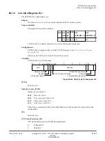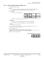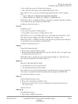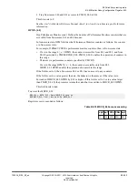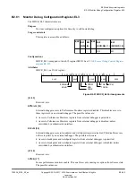
This field is RO.
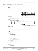
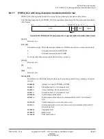
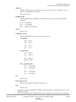
SCU-L2 Cache Protection, [21]
SCU-L2 Cache Protection. L2 cache is implemented:
0
Without ECC.
1
With ECC.
This field is RO.
[20:6]
Reserved,
RES0
.
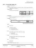
L2 data RAM input latency, [5]
L2 data RAM input latency:
0
1-cycle input delay from L2 data RAMs.
1
2-cycle input delay from L2 data RAMs.
This field is RO.
[4:1]
Reserved,
RES0
.
L2 data RAM output latency, [0]
L2 data RAM output latency:
0
2-cycle output delay from L2 data RAMs.
1
3-cycle output delay from L2 data RAMs.
This field is RO.
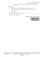
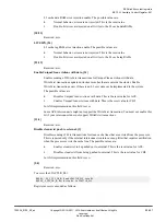
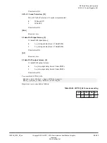
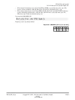
To access the L2CTLR_EL1:
MRS <Xt>, S3_1_C11_C0_2 ; Read L2CTLR_EL1 into Xt
MSR S3_1_C11_C0_2, <Xt>; Write Xt to L2CTLR_EL1
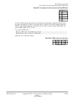
Register access is encoded as follows:
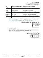
Table B2-65 L2CTLR_EL1 access encoding
op0 op1 CRn CRm op2
11
001 1011 0000 010
B2 AArch64 system registers
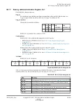
B2.74 L2 Control Register, EL1
100236_0100_00_en
Copyright © 2015–2017, 2019 Arm Limited or its affiliates. All rights
reserved.
B2-490
Non-Confidential
Summary of Contents for Cortex-A35
Page 4: ......
Page 18: ......
Page 26: ......
Page 27: ...Part A Functional Description ...
Page 28: ......
Page 145: ...Part B Register Descriptions ...
Page 146: ......
Page 573: ...Part C Debug ...
Page 574: ......
Page 845: ...Part D Appendices ...
Page 846: ......


