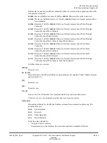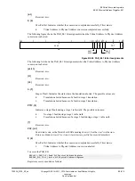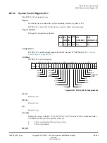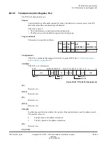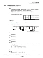
RES0
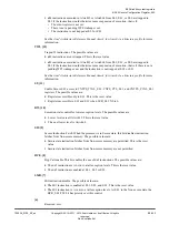
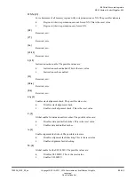
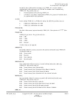
T32EE is not implemented.
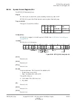
CP15BEN, [5]
CP15 barrier enable. The possible values are:
0
CP15 barrier operations disabled. Their encodings are
UNDEFINED
.
1
CP15 barrier operations enabled. This is the reset value.
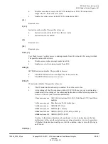
SA0, [4]
Enable EL0 stack alignment check. The possible values are:
0
Disable EL0 stack alignment check.
1
Enable EL0 stack alignment check. This is the reset value.
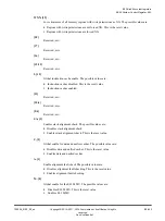
SA, [3]
Enable SP alignment check. The possible values are:
0
Disable SP alignment check.
1
Enable SP alignment check. This is the reset value.
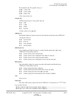
C, [2]
Cache enable. The possible values are:
0
Data and unified caches disabled. This is the reset value.
1
Data and unified caches enabled.
A, [1]
Alignment check enable. The possible values are:
0
Alignment fault checking disabled. This is the reset value.
1
Alignment fault checking enabled.
M, [0]
MMU enable. The possible values are:
0
EL1 and EL0 stage 1 MMU disabled. This is the reset value.
1
EL1 and EL0 stage 1 MMU enabled.
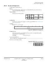
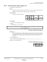
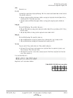
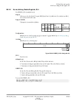
To access the SCTLR_EL1:
MRS <Xt>, SCTLR_EL1 ; Read SCTLR_EL1 into Xt
MSR SCTLR_EL1, <Xt> ; Write Xt to SCTLR_EL1
Register access is encoded as follows:
Table B2-84 SCTLR_EL1 access encoding
op0 op1 CRn CRm op2
11
000 0001 0000 000
B2 AArch64 system registers
B2.90 System Control Register, EL1
100236_0100_00_en
Copyright © 2015–2017, 2019 Arm Limited or its affiliates. All rights
reserved.
B2-528
Non-Confidential
Summary of Contents for Cortex-A35
Page 4: ......
Page 18: ......
Page 26: ......
Page 27: ...Part A Functional Description ...
Page 28: ......
Page 145: ...Part B Register Descriptions ...
Page 146: ......
Page 573: ...Part C Debug ...
Page 574: ......
Page 845: ...Part D Appendices ...
Page 846: ......


