B1.91
L2 Auxiliary Control Register
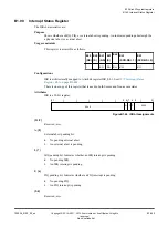
The L2ACTLR characteristics are:
Purpose
Provides configuration and control options for the L2 memory system.
Usage constraints
This register is accessible as follows:
EL0
(NS)
EL0
(S)
EL1
(NS)
EL1
(S)
EL2 EL3
(SCR.NS = 1)
EL3
(SCR.NS = 0)
-
-
RW
RW RW RW
RW
You can write to this register only when the L2 memory system is idle. Arm recommends that
you write to this register after a powerup reset before the MMU is enabled and before any AXI,
ACE, CHI, or ACP traffic has begun.
If the register must be modified after a powerup reset sequence, to idle the L2 memory system,
you must take the following steps:
1. Disable the MMU from each core followed by an ISB to ensure the MMU disable operation
is complete, then followed by a DSB to drain previous memory transactions.
2. Ensure that the system has no outstanding AC channel coherence requests to the Cortex
‑
A35
processor.
3. Ensure that the system has no outstanding ACP requests to the Cortex
‑
A35 processor.
When the L2 is idle, the processor can update the L2ACTLR followed by an
ISB
. After the
L2ACTLR is updated, the MMUs can be enabled and normal ACE and ACP traffic can resume.
Configurations
There is one copy of this register that is used in both Secure and Non-secure states.
L2ACTLR is mapped to the AArch64 L2ACTLR_EL1 register. See
Attributes
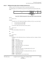
L2ACTLR is a 32-bit register.
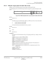
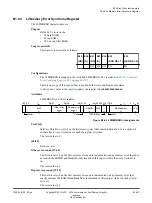
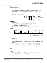
31 30 29
15 14 13
4 3 2
0
RES
0
RES
0
Disable clean/evict push to external
Enable UniqueClean evictions with data
L2 Victim Control
RES
0
L2DEIEN
28
25 24
RES
0
L2TEIEN
Figure B1-45 L2ACTLR bit assignments
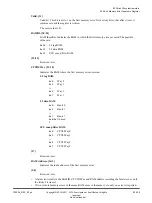
[31:30]
L2 Victim Control.
0b10
This is the default value. Software must not change it.
L2DEIEN, [29]
L2 cache data RAM error injection enable. The possible values are:
0
Normal behavior, errors are not injected. This is the reset value.
B1 AArch32 system registers
B1.91 L2 Auxiliary Control Register
100236_0100_00_en
Copyright © 2015–2017, 2019 Arm Limited or its affiliates. All rights
reserved.
B1-301
Non-Confidential
Summary of Contents for Cortex-A35
Page 4: ......
Page 18: ......
Page 26: ......
Page 27: ...Part A Functional Description ...
Page 28: ......
Page 145: ...Part B Register Descriptions ...
Page 146: ......
Page 573: ...Part C Debug ...
Page 574: ......
Page 845: ...Part D Appendices ...
Page 846: ......

