A2.1
Components
The Cortex
‑
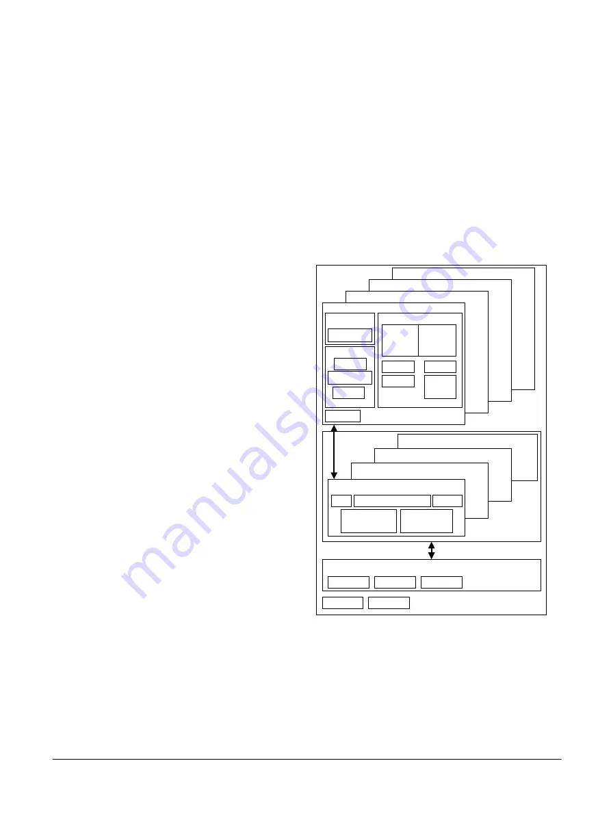
A35 processor consists of:
• One to four cores, each with its own governor block. The governor block provides functionality that
remains required when the core is in retention.
• An SCU-L2 memory system block. The SCU maintains data coherency between the L1 data caches
and the L2 cache. It also connects the cores to an external memory system using an AXI, ACE, or
CHI master interface. A mini-SCU replaces the SCU in configurations that do not require the SCU
functionality. The mini-SCU is instantiated in implementations that are configured with a single core,
no L2 cache, no CPU cache protection, and an AXI master interface.
The processor also integrates CoreSight components, and optionally integrates cache protection and the
Cryptographic Extension.
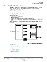
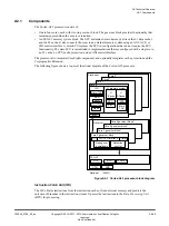
The following figure shows a top-level functional diagram of the Cortex
‑
A35 processor.
Core 1 governor block*
Core 3*
Core 2*
ETM
Core 0
GIC CPU interface*
CTI
SCU-L2
ACP*
Processor
Timer
CTM
APB
L2 cache*
Core 1*
Governor
Core 0 governor block
IFU
Micro-TLB
+
SCU
Core 2 governor block*
Core 3 governor block*
ETM*
DPU
PMU
Micro-TLB
+
Neon*
L1 memory system
L1
ICache
L1
DCache
DCU
STB
BIU
Main
TLB
+
*Optional
Debug over
powerdown
Retention
control
+
MMU
Figure A2-1 Cortex-A35 processor block diagram
Instruction Fetch Unit (IFU)
The IFU obtains instructions from the instruction cache or from external memory and predicts the
outcome of branches in the instruction stream. It passes the instructions to the
Data Processing Unit
(DPU) for processing.
A2 Technical Overview
A2.1 Components
100236_0100_00_en
Copyright © 2015–2017, 2019 Arm Limited or its affiliates. All rights
reserved.
A2-40
Non-Confidential
Summary of Contents for Cortex-A35
Page 4: ......
Page 18: ......
Page 26: ......
Page 27: ...Part A Functional Description ...
Page 28: ......
Page 145: ...Part B Register Descriptions ...
Page 146: ......
Page 573: ...Part C Debug ...
Page 574: ......
Page 845: ...Part D Appendices ...
Page 846: ......


