Clocking and Resets
6-2
Copyright © 2005-2008 ARM Limited. All rights reserved.
ARM DDI 0337G
Non-Confidential
Unrestricted Access
6.1
Clocking
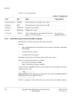
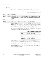
The processor has three functional clock inputs. Table 6-1 describes the processor
clocks.
FCLK
and
HCLK
are synchronous to each other.
FCLK
is a free running version of
HCLK
, and therefore must always be the same frequency when not in sleep mode. For
more information, see Chapter 7
Power Management
.
FCLK
and
HCLK
must be
balanced with respect to each other, with equal latencies into the processor.
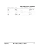
The processor is integrated with components for debug and trace. Your macrocell might
contain some, or all, of the clocks shown in Table 6-2.
SWCLKTCK
is the clock for the debug interface domain of the SWJ-DP. In JTAG
mode this is equivalent to
TCK
. In Serial Wire Mode this is the Serial Wire clock. It is
asynchronous to all other clocks.
DBGCLK
is the clock for the debug interface domain
of SW-DP. It is asynchronous to the other clocks.
TRACECLKIN
is the reference clock for the
Trace Port Interface Unit
(TPIU). It is
asynchronous to the other clocks.
Table 6-1 Cortex-M3 processor clocks
Clock
Domain
Description
FCLK
Processor
Free running processor clock, used for sampling interrupts and clocking debug blocks.
FCLK
ensures that interrupts can be sampled, and sleep events can be traced, while the processor is
sleeping.
HCLK
Processor
Processor clock.
DAPCLK
Processor
Debug port
Advanced High-performance Bus Access Port
(AHB-AP) clock.
Table 6-2 Cortex-M3 macrocell clocks
Clock
Domain
Description
TRACECLKIN
TPIU
Clocks the output of the TPIU
DBGCLK
SW-DP
Debug clock
SWCLKTCK
SWJ-DP
Debug
clock


